SLOS369G July   2002  – October 2015 TPA2005D1

PRODUCTION DATA.  

  1. Features
  2. Applications
  3. Description
  4. Revision History
  5. Device Comparison Table
  6. Pin Configuration and Functions
  7. Specifications
    1. 7.1 Absolute Maximum Ratings
    2. 7.2 ESD Ratings
    3. 7.3 Recommended Operating Conditions
    4. 7.4 Thermal Information
    5. 7.5 Electrical Characteristics
    6. 7.6 Operating Characteristics
    7. 7.7 Typical Characteristics
  8. Parameter Measurement Information
  9. Detailed Description
    1. 9.1 Overview
    2. 9.2 Functional Block Diagram
    3. 9.3 Feature Description
      1. 9.3.1 Fully Differential Amplifier
        1. 9.3.1.1 Advantages of Fully Differential Amplifiers
      2. 9.3.2 Efficiency and Thermal Information
      3. 9.3.3 Eliminating the Output Filter with the TPA2005D1
        1. 9.3.3.1 Effect on Audio
        2. 9.3.3.2 Traditional Class-D Modulation Scheme
        3. 9.3.3.3 TPA2005D1 Modulation Scheme
        4. 9.3.3.4 Efficiency: Why You Must Use a Filter With the Traditional Class-D Modulation Scheme
        5. 9.3.3.5 Effects of Applying a Square Wave Into a Speaker
        6. 9.3.3.6 When to Use an Output Filter
      4. 9.3.4 Thermal and Short-Circuit Protection
    4. 9.4 Device Functional Modes
      1. 9.4.1 Summing Input Signals with the TPA2005D1
        1. 9.4.1.1 Summing Two Differential Input Signals
        2. 9.4.1.2 Summing a Differential Input Signal and a Single-Ended Input Signal
        3. 9.4.1.3 Summing Two Single-Ended Input Signals
      2. 9.4.2 Shutdown Mode
  10. 10Application and Implementation
    1. 10.1 Application Information
    2. 10.2 Typical Applications
      1. 10.2.1 TPA2005D1 with Differential Input
        1. 10.2.1.1 Design Requirements
        2. 10.2.1.2 Detailed Design Procedure
          1. 10.2.1.2.1 Component Selection
          2. 10.2.1.2.2 Input Resistors (RI)
          3. 10.2.1.2.3 Decoupling Capacitor (CS)
        3. 10.2.1.3 Application Curves
      2. 10.2.2 TPA2005D1 with Differential Input and Input Capacitors
        1. 10.2.2.1 Design Requirements
        2. 10.2.2.2 Detailed Design Procedure
          1. 10.2.2.2.1 Input Capacitors (CI)
      3. 10.2.3 TPA2005D1 with Single-Ended Input
        1. 10.2.3.1 Design Requirements
        2. 10.2.3.2 Detailed Design Procedure
  11. 11Power Supply Recommendations
    1. 11.1 Power Supply Decoupling Capacitors
  12. 12Layout
    1. 12.1 Layout Guidelines
      1. 12.1.1 Component Location
      2. 12.1.2 Trace Width
      3. 12.1.3 MicroStar Junior™ BGA Specifications
    2. 12.2 Layout Examples
  13. 13Device and Documentation Support
    1. 13.1 Community Resources
    2. 13.2 Trademarks
    3. 13.3 Electrostatic Discharge Caution
    4. 13.4 Glossary
  14. 14Mechanical, Packaging, and Orderable Information

Package Options

Refer to the PDF data sheet for device specific package drawings

Mechanical Data (Package|Pins)
  • DGN|8
  • DRB|8
Thermal pad, mechanical data (Package|Pins)
Orderable Information

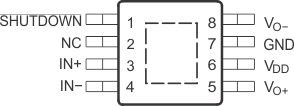
6 Pin Configuration and Functions

GQY and ZQY Packages
15-Pin MicroStar Junior™
Top and Side Views
TPA2005D1 po_msj_top_side_slos369.gif
DRB Package
8-Pin VSON
Top View
TPA2005D1 po_drb_pckg_top_slos369.gif
DGN Package
8-Pin HVSSOP
Top View
TPA2005D1 po_dgn_pckg_top_slos369.gif
A. The shaded terminals are used for electrical and thermal connections to the ground plane. All the shaded terminals need to be electrically connected to ground. No connect (NC) terminals still need a pad and trace.
B. The thermal pad of the DRB and DGN packages must be electrically and thermally connected to a ground plane.

Pin Functions

PIN I/O DESCRIPTION
NAME GQY, ZQY DRB, DGN
GND A2, A3, B3, C2, C3, D2, D3 7 I High-current ground
IN- D1 4 I Negative differential input
IN+ C1 3 I Positive differential input
NC B1 2 No internal connection
SHUTDOWN A1 1 I Shutdown terminal (active low logic)
Thermal Pad Must be soldered to a grounded pad on the PCB.
VDD B4, C4 6 I Power supply
VO- A4 8 O Negative BTL output
VO+ D4 5 O Positive BTL output