SLOS626B December 2009 – November 2015 TPA2011D1
PRODUCTION DATA.
- 1 Features
- 2 Applications
- 3 Description
- 4 Revision History
- 5 Device Comparison Table
- 6 Pin Configuration and Functions
- 7 Specifications
- 8 Parameter Measurement Information
- 9 Detailed Description
- 10Application and Implementation
- 11Power Supply Recommendations
- 12Layout
- 13Device and Documentation Support
- 14Mechanical, Packaging, and Orderable Information
Package Options
Mechanical Data (Package|Pins)
- YFF|9
Thermal pad, mechanical data (Package|Pins)
Orderable Information
9 Detailed Description
9.1 Overview
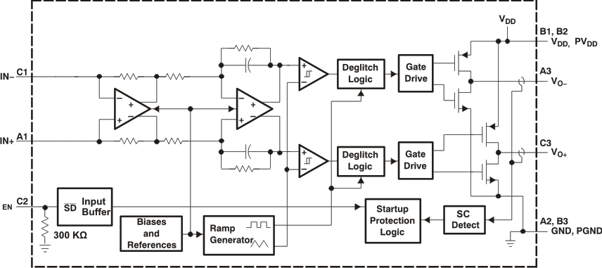
The TPA2011D1 is a high-efficiency filter-free Class-D audio amplifier capable of delivering up to 3.2W into 4-Ω load with 5-V power supply. The fully-differential design of this amplifier avoids the usage of bypass capacitors and the improved CMRR eliminates the usage of input-coupling capacitors. This makes the device size a perfect choice for small, portable applications as only three external components are required. The advanced modulation used in the TPA2011D1 PWM output stage eliminates the need for an output filter.
9.2 Functional Block Diagram
9.3 Feature Description
9.3.1 Fully Differential Amplifier
The TPA2011D1 is a fully differential amplifier with differential inputs and outputs. The fully differential amplifier consists of a differential amplifier and a common-mode amplifier. The differential amplifier ensures that the amplifier outputs a differential voltage on the output that is equal to the differential input times the gain. The common-mode feedback ensures that the common-mode voltage at the output is biased around VDD/2 regardless of the common-mode voltage at the input. The fully differential TPA2011D1 can still be used with a single-ended input; however, the TPA2011D1 should be used with differential inputs when in a noisy environment, like a wireless handset, to ensure maximum noise rejection.
9.3.1.1 Advantages of Fully Differential Amplifiers
- Input-coupling Capacitors Not Required
- The fully differential amplifier allows the inputs to be biased at voltage other than mid-supply. For example, if a codec has a midsupply lower than the midsupply of the TPA2011D1, the common-mode feedback circuit will adjust, and the TPA2011D1 outputs will still be biased at midsupply of the TPA2011D1. The inputs of the TPA2011D1 can be biased from 0.5 V to VDD –0.8 V. If the inputs are biased outside of that range, input-coupling capacitors are required.
- Midsupply Bypass Capacitor, C(BYPASS), Not Required
- The fully differential amplifier does not require a bypass capacitor. This is because any shift in the midsupply affects both positive and negative channels equally and cancels at the differential output.
- Better RF-Immunity
- GSM handsets save power by turning on and shutting off the RF transmitter at a rate of 217 Hz. The transmitted signal is picked-up on input and output traces. The fully differential amplifier cancels the signal much better than the typical audio amplifier.
9.3.2 Eliminating the Output Filter With the TPA2011D1
This section focuses on why the user can eliminate the output filter with the TPA2011D1.
9.3.2.1 Effect on Audio
The class-D amplifier outputs a pulse-width modulated (PWM) square wave, which is the sum of the switching waveform and the amplified input audio signal. The human ear acts as a band-pass filter such that only the frequencies between approximately 20 Hz and 20 kHz are passed. The switching frequency components are much greater than 20 kHz, so the only signal heard is the amplified input audio signal.
9.3.2.2 When to Use an Output Filter
Design the TPA2011D1 without an Inductor / Capacitor (LC) output filter if the traces from the amplifier to the speaker are short. Wireless handsets and PDAs are great applications for this class-D amplifier to be used without an output filter.
The TPA2011D1 does not require an LC output filter for short speaker connections (approximately 100 mm long or less). A ferrite bead can often be used in the design if failing radiated emissions testing without an LC filter; and, the frequency-sensitive circuit is greater than 1 MHz. If choosing a ferrite bead, choose one with high impedance at high frequencies, but very low impedance at low frequencies. The selection must also take into account the currents flowing through the ferrite bead. Ferrites can begin to loose effectiveness at much lower than rated current values. See the TPA2011D1 EVM User's Guide for components used successfully by TI.
Figure 29 shows a typical ferrite-bead output filter.
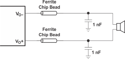 Figure 29. Typical Ferrite Chip Bead Filter
9.3.3 Short Circuit Auto-Recovery
When a short-circuit event occurs, the TPA2011D1 goes to shutdown mode and activates the integrated auto-recovery process whose aim is to return the device to normal operation once the short-circuit is removed. This process repeatedly examines (once every 100ms) whether the short-circuit condition persists, and returns the device to normal operation immediately after the short-circuit condition is removed. This feature helps protect the device from large currents and maintain a good long-term reliability.
9.3.4 Integrated Image Reject Filter for DAC Noise Rejection
In applications which use a DAC to drive Class-D amplifiers, out-of-band noise energy present at the DAC's image frequencies fold back into the audio-band at the output of the Class-D amplifier. An external low-pass filter is often placed between the DAC and the Class-D amplifier in order to attenuate this noise.
The TPA2011D1 has an integrated Image Reject Filter with a low-pass cutoff frequency of 130 kHz, which significantly attenuates this noise. Depending on the system noise specification, the integrated Image Reject Filter may help eliminate external filtering, thereby saving board space and component cost.
9.4 Device Functional Modes
9.4.1 Summing Input Signals With the TPA2011D1
Most wireless phones or PDAs need to sum signals at the audio power amplifier or just have two signal sources that need separate gain. The TPA2011D1 makes it easy to sum signals or use separate signal sources with different gains. Many phones now use the same speaker for the earpiece and ringer, where the wireless phone would require a much lower gain for the phone earpiece than for the ringer. PDAs and phones that have stereo headphones require summing of the right and left channels to output the stereo signal to the mono speaker.
9.4.1.1 Summing Two Differential Input Signals
Two extra resistors are needed for summing differential signals (a total of 5 components). The gain for each input source can be set independently (see Equation 1 and Equation 2, and Figure 30).


If summing left and right inputs with a gain of 1 V/V, use RI1 = RI2 = 300 kΩ.
If summing a ring tone and a phone signal, set the ring-tone gain to Gain 2 = 2 V/V, and the phone gain to gain 1 = 0.1 V/V. The resistor values would be:
RI1 = 3 MΩ, and = RI2 = 150 kΩ.
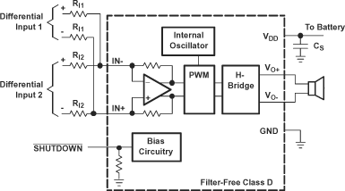 Figure 30. Application Schematic With TPA2011D1 Summing Two Differential Inputs
9.4.1.2 Summing a Differential Input Signal and a Single-Ended Input Signal
Figure 31 shows how to sum a differential input signal and a single-ended input signal. Ground noise can couple in through IN+ with this method. It is better to use differential inputs. The corner frequency of the single-ended input is set by CI2, shown in Equation 5. To assure that each input is balanced, the single-ended input must be driven by a low-impedance source even if the input is not in use


If summing a ring tone and a phone signal, the phone signal should use a differential input signal while the ring tone might be limited to a single-ended signal. Phone gain is set at gain 1 = 0.1 V/V, and the ring-tone gain is set to gain 2 = 2 V/V, the resistor values would be…
RI1 = 3 MΩ, and = RI2 = 150 kΩ.
The high pass corner frequency of the single-ended input is set by CI2. If the desired corner frequency is less than 20 Hz...


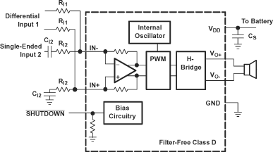 Figure 31. Application Schematic With TPA2011D1 Summing Differential Input and Single-Ended Input Signals
9.4.1.3 Summing Two Single-Ended Input Signals
Four resistors and three capacitors are needed for summing single-ended input signals. The gain and corner frequencies (fc1 and fc2) for each input source can be set independently (see Equation 8 through Equation 11, and Figure 32). Resistor, RP, and capacitor, CP, are needed on the IN+ terminal to match the impedance on the IN– terminal. The single-ended inputs must be driven by low impedance sources even if one of the inputs is not outputting an ac signal.


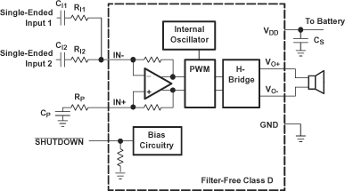 Figure 32. Application Schematic With TPA2011D1 Summing Two Single-Ended Inputs
9.4.2 Shutdown Mode
The TPA2011D1 can be put in shutdown mode when asserting SHUTDOWN pin to a logic LOW. While in shutdown mode, the device output stage is turned off and set into high impedance, making the current consumption very low. The device exits shutdown mode when a HIGH logic level is applied to SHUTDOWN pin.