SLOS524E June   2008  – May 2016 TPA2016D2

PRODUCTION DATA.  

  1. Features
  2. Applications
  3. Description
  4. Revision History
  5. Device Comparison Table
  6. Pin Configuration and Functions
  7. Specifications
    1. 7.1 Absolute Maximum Ratings
    2. 7.2 ESD Ratings
    3. 7.3 Recommended Operating Conditions
    4. 7.4 Thermal Information
    5. 7.5 Electrical Characteristics
    6. 7.6 I2C Timing Requirements
    7. 7.7 Dissipation Ratings
    8. 7.8 Operating Characteristics
    9. 7.9 Typical Characteristics
  8. Parameter Measurement Information
  9. Detailed Description
    1. 9.1 Overview
    2. 9.2 Functional Block Diagram
    3. 9.3 Feature Description
      1. 9.3.1 Operation With DACs and CODECs
      2. 9.3.2 Filter-Free Operation and Ferrite Bead Filters
      3. 9.3.3 Short-Circuit Protection
      4. 9.3.4 Automatic Gain Control
        1. 9.3.4.1 Fixed Gain
        2. 9.3.4.2 Limiter Level
        3. 9.3.4.3 Compression Ratio
        4. 9.3.4.4 Interaction Between Compression Ratio and Limiter Range
        5. 9.3.4.5 Noise Gate Threshold
        6. 9.3.4.6 Maximum Gain
        7. 9.3.4.7 Attack, Release, and Hold Time
    4. 9.4 Device Functional Modes
      1. 9.4.1 TPA2016D2 AGC Operation
      2. 9.4.2 TPA2016D2 AGC Recommended Settings
    5. 9.5 Programming
      1. 9.5.1 General I2C Operation
      2. 9.5.2 Single- and Multiple-Byte Transfers
      3. 9.5.3 Single-Byte Write
      4. 9.5.4 Multiple-Byte Write and Incremental Multiple-Byte Write
      5. 9.5.5 Single-Byte Read
      6. 9.5.6 Multiple-Byte Read
    6. 9.6 Register Maps
  10. 10Application and Implementation
    1. 10.1 Application Information
    2. 10.2 Typical Applications
      1. 10.2.1 TPA2016D2 With Differential Input Signal
        1. 10.2.1.1 Design Requirements
        2. 10.2.1.2 Detailed Design Procedure
          1. 10.2.1.2.1 Surface Mount Capacitors
          2. 10.2.1.2.2 Decoupling Capacitor, CS
          3. 10.2.1.2.3 Input Capacitors, CI
        3. 10.2.1.3 Application Curves
      2. 10.2.2 TPA2016D2 With Single-Ended Input Signal
        1. 10.2.2.1 Design Requirements
        2. 10.2.2.2 Detailed Design Procedure
        3. 10.2.2.3 Application Curves
  11. 11Power Supply Recommendations
    1. 11.1 Power Supply Decoupling Capacitors
  12. 12Layout
    1. 12.1 Layout Guidelines
      1. 12.1.1 Component Location
      2. 12.1.2 Trace Width
      3. 12.1.3 Pad Side
    2. 12.2 Layout Examples
    3. 12.3 Efficiency and Thermal Considerations
  13. 13Device and Documentation Support
    1. 13.1 Device Support
      1. 13.1.1 Third-Party Products Disclaimer
    2. 13.2 Community Resources
    3. 13.3 Trademarks
    4. 13.4 Electrostatic Discharge Caution
    5. 13.5 Glossary
  14. 14Mechanical, Packaging, and Orderable Information

Package Options

Mechanical Data (Package|Pins)
Thermal pad, mechanical data (Package|Pins)
Orderable Information

8 Parameter Measurement Information

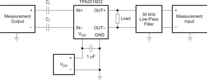
All parameters are measured according to the conditions described in Specifications. Figure 25 shows the setup used for the typical characteristics of the test device.
TPA2016D2 test_los524.gif
1. All measurements were taken with a 1-μF CI (unless otherwise noted.)
2. A 33-μH inductor was placed in series with the load resistor to emulate a small speaker for efficiency measurements.
3. The 30-kHz low-pass filter is required, even if the analyzer has an internal low-pass filter. An RC low-pass filter (1 kΩ 4.7 nF) is used on each output for the data sheet graphs.
4. All THD + N graphs are taken with outputs out of phase (unless otherwise noted). All data is taken on left channel.
5. All data is taken on the DSBGA package unless otherwise noted.
Figure 25. Test Setup for Graphs