SLOS660C January   2010  – October 2015 TPA2028D1

PRODUCTION DATA.  

  1. Features
  2. Applications
  3. Description
  4. Revision History
  5. Device Comparison Table
  6. Pin Configuration and Functions
  7. Specifications
    1. 7.1 Absolute Maximum Ratings
    2. 7.2 ESD Ratings
    3. 7.3 Recommended Operating Conditions
    4. 7.4 Thermal Information
    5. 7.5 Electrical Characteristics
    6. 7.6 Operating Characteristics
    7. 7.7 I2C Timing Requirements
    8. 7.8 Typical Characteristics
  8. Parameter Measurement Information
  9. Detailed Description
    1. 9.1 Overview
    2. 9.2 Functional Block Diagram
    3. 9.3 Feature Description
      1. 9.3.1 Automatic Gain Control
      2. 9.3.2 Operation With DACs and CODECs
      3. 9.3.3 Filter Free Operation and Ferrite Bead Filters
      4. 9.3.4 General I2C Operation
        1. 9.3.4.1 Single- and Multiple-Byte Transfers
        2. 9.3.4.2 Single-Byte Write
        3. 9.3.4.3 Multiple-Byte Write and Incremental Multiple-Byte Write
        4. 9.3.4.4 Single-Byte Read
        5. 9.3.4.5 Multiple-Byte Read
    4. 9.4 Device Functional Modes
      1. 9.4.1 Enable/Disable Amplifier
      2. 9.4.2 TPA2028D1 AGC and Start-Up Operation
        1. 9.4.2.1 AGC Startup Condition
      3. 9.4.3 Short Circuit Auto-Recovery
    5. 9.5 Programming
      1. 9.5.1 TPA2028D1 AGC Recommended Settings
    6. 9.6 Register Maps
  10. 10Application and Implementation
    1. 10.1 Application Information
    2. 10.2 Typical Application
      1. 10.2.1 Design Requirements
      2. 10.2.2 Detailed Design Procedure
        1. 10.2.2.1 Decoupling Capacitor CS
        2. 10.2.2.2 Input Capacitors CI)
      3. 10.2.3 Application Curves
  11. 11Power Supply Recommendations
    1. 11.1 Power Supply Decoupling Capacitors
  12. 12Layout
    1. 12.1 Layout Guidelines
      1. 12.1.1 Component Placement
      2. 12.1.2 Trace Width
      3. 12.1.3 Pad Size
    2. 12.2 Layout Example
    3. 12.3 Efficiency and Thermal Considerations
  13. 13Device and Documentation Support
    1. 13.1 Device Support
      1. 13.1.1 Third-Party Products Disclaimer
    2. 13.2 Community Resources
    3. 13.3 Trademarks
    4. 13.4 Electrostatic Discharge Caution
    5. 13.5 Glossary
  14. 14Mechanical, Packaging, and Orderable Information

Package Options

Mechanical Data (Package|Pins)
Thermal pad, mechanical data (Package|Pins)
Orderable Information

6 Pin Configuration and Functions

YZF Package
9-Pin DSBGA
Top View
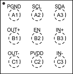
TPA2028D1 pinout2_los592.gif

Pin Functions

PIN I/O/P(1) DESCRIPTION
NAME NO.
EN B2 I Enable terminal (active high)
IN+ B3 I Positive audio input
IN– C3 I Negative audio input
OUT+ B1 O Positive differential output
OUT– C1 O Negative differential output
PGND A1 P Power ground
PVDD C2 P Power supply
SCL A2 I I2C clock interface
SDA A3 I/O I2C data interface
(1) I = Input, O = Output, P = Power