SLOS618F August 2009 – July 2016 TPA3111D1
PRODUCTION DATA.
- 1 Features
- 2 Applications
- 3 Description
- 4 Revision History
- 5 Pin Configuration and Functions
- 6 Specifications
- 7 Detailed Description
-
8 Application and Implementation
- 8.1 Application Information
- 8.2
Typical Application
- 8.2.1 Design Requirements
- 8.2.2
Detailed Design Procedure
- 8.2.2.1 Ferrite Bead Filter Considerations
- 8.2.2.2 Efficiency: LC Filter Required With the Traditional Class-D Modulation Scheme
- 8.2.2.3 When to Use an Output Filter for EMI Suppression
- 8.2.2.4 Input Resistance
- 8.2.2.5 Input Capacitor, CI
- 8.2.2.6 BSN and BSP Capacitors
- 8.2.2.7 Differential Inputs
- 8.2.2.8 Using Low-ESR Capacitors
- 8.2.3 Application Curves
- 9 Power Supply Recommendations
- 10Layout
- 11Device and Documentation Support
- 12Mechanical, Packaging, and Orderable Information
Package Options
Mechanical Data (Package|Pins)
- PWP|28
Thermal pad, mechanical data (Package|Pins)
- PWP|28
Orderable Information
7 Detailed Description
7.1 Overview
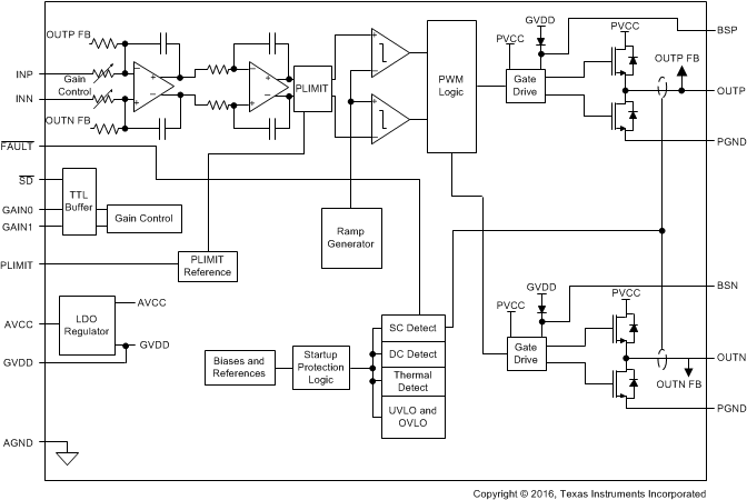
To facilitate system design, the TPA3111D1 requires only a single power supply from 8 V to 26 V for operation. An internal voltage regulator provides suitable voltage levels for the gate driver, digital and low-voltage analog circuitry. Additionally, all circuitry requiring a floating voltage supply, that is, the high-side gate drive, is accommodated by built-in bootstrap circuitry with integrated bootstrap diodes requiring only an external capacitor for each half-bridge. The audio signal path, including the gate drive and output stage is designed as identical, independent full-bridges. Place all decoupling capacitors as close to their associated pins as possible. In general, the physical loop with the power supply pins, decoupling capacitors and GND return path to the device pins must be kept as short as possible and with as little area as possible to minimize induction (see TPA3111D1 Evaluation Module for additional information).
For a properly functioning bootstrap circuit, a small ceramic capacitor must be connected from each bootstrap pin (BSx) to the power-stage output pin (OUTx). When the power-stage output is low, the bootstrap capacitor is charged through an internal diode connected between the gate-drive power-supply pin (GVDD) and the bootstrap pins. When the power-stage output is high, the bootstrap capacitor potential is shifted above the output potential and thus provides a suitable voltage supply for the high-side gate driver. In an application with PWM switching frequencies approximately 310 kHz, TI recommends ceramic capacitors with at least 220-nF capacitance, size 0603 or 0805, for the bootstrap supply. These capacitors ensure sufficient energy storage, even during clipped low frequency audio signals, to keep the high-side power stage FET (LDMOS) fully turned on during the remaining part of its ON cycle. Pay special attention to the power-stage power supply; this includes component selection, PCB placement, and routing. For optimal electrical performance, EMI compliance, and system reliability, it is important that each PVCC pin is decoupled with ceramic capacitors placed as close as possible to each supply pin. TI recommends following the PCB layout of the TPA3111D1 EVM. For additional information on recommended power supply and required components, see Application and Implementation and Power Supply Recommendations. The PVCC power supply must have low output impedance and low noise. The power-supply ramp and SD release sequence is not critical for device reliability as facilitated by the internal power-on-reset circuit, but TI recommends releasing SD after the power supply is settled for minimum turnon audible artifacts.
7.2 Functional Block Diagram

7.3 Feature Description
7.3.1 Gain Setting Through GAIN0 and GAIN1 Inputs
The gain of the TPA3111D1 is set by two input pins, GAIN0 and GAIN1. The voltage slew rate of these gain pins, along with SD and AVCC (pin 14), must be restricted to no more than 10 V/ms. For higher slew rates, use a 100-kΩ resistor in series with the pins.
The gains listed in Table 1 are realized by changing the taps on the input resistors inside the amplifier. This causes the input impedance (ZI) to be dependent on the gain setting. The actual gain settings are controlled by ratios of resistors, so the gain variation from part-to-part is small. However, the input impedance from part to part at the same gain may shift by ±20% due to shifts in the actual resistance of the input resistors.
For design purposes, the input network must be designed assuming an input impedance of 7.2 kΩ, which is the absolute minimum input impedance of the TPA3111D1. At the lower gain settings, the input impedance could increase as high as 72 kΩ
Table 1. Gain Setting
| GAIN1 | GAIN0 | AMPLIFIER GAIN (dB) | INPUT IMPEDANCE (kΩ) |
|---|---|---|---|
| TYPICAL | TYPICAL | ||
| 0 | 0 | 20 | 60 |
| 0 | 1 | 26 | 30 |
| 1 | 0 | 32 | 15 |
| 1 | 1 | 36 | 9 |
7.3.2 SD Operation
The TPA3111D1 employs a shutdown mode of operation designed to reduce supply current (ICC) to the absolute minimum level during periods of nonuse for power conservation. The SD input pin must be held high (see specification table for trip point) during normal operation when the amplifier is in use. Pulling SD low causes the outputs to mute and the amplifier to enter a low-current state. Never leave SD unconnected, because amplifier operation would be unpredictable.
For the best power-off pop performance, place the amplifier in the shutdown mode before removing the power supply voltage.
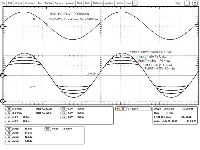
7.3.3 PLIMIT
The voltage at pin 10 can used to limit the power to levels less than what is possible based on the supply rail. Add a resistor divider from GVDD to ground to set the voltage at the PLIMIT pin. An external reference may also be used if tighter tolerance is required. Also add a 1-µF capacitor from pin 10 to ground.
The PLIMIT circuit sets a limit on the output peak-to-peak voltage. This limit can be thought of as a virtual voltage rail which is lower than the supply connected to PVCC. This virtual rail is 4 times the voltage at the PLIMIT pin. This output voltage can be used to calculate the maximum output power for a given maximum input voltage and speaker impedance.
 Figure 15. PLIMIT Circuit Operation
The PLIMIT circuits sets a limit on the output peak-to-peak voltage. The limiting is done by limiting the duty cycle to fixed maximum value. This limit can be thought of as a virtual voltage rail which is lower than the supply connected to PVCC. This virtual rail is 4 times the voltage at the PLIMIT pin. This output voltage can be used to calculate the maximum output power for a given maximum input voltage and speaker impedance.

where
- RS is the total series resistance including RDS(on), and any resistance in the output filter.
- RL is the load resistance.
- VP is the peak amplitude of the output possible within the supply rail.
- VP = 4 × PLIMIT voltage if PLIMIT < 4 × VP
- POUT(10%THD) = 1.25 × POUT(unclipped)
Table 2. PLIMIT Typical Operation
| TEST CONDITIONS | PLIMIT VOLTAGE | OUTPUT POWER (W) |
OUTPUT VOLTAGE AMPLITUDE (VP-P) |
|---|---|---|---|
| VCC = 24 V, VIN=1 Vrms, RL = 4 Ω, Gain=20 dB |
1.92 | 10 | 15 |
| VCC = 24 V, VIN = 1 Vrms, RL = 4 Ω, Gain = 20 dB |
1.24 | 5 | 10 |
| VCC = 12 V , VIN = 1 Vrms, RL = 4 Ω, Gain = 20 dB |
1.75 | 10 | 15.3 |
| VCC = 12 V, VIN = 1 Vrms, RL = 4 Ω, Gain = 20 dB |
1.2 | 5 | 10.3 |
7.3.4 GVDD Supply
The GVDD supply is used to power the gates of the output full bridge transistors. It can also used to supply the PLIMIT voltage divider circuit. Add a 1-µF capacitor to ground at this pin.
7.3.5 DC Detect
TPA3111D1 has circuitry which protects the speakers from DC current that might occur due to defective capacitors on the input or shorts on the printed-circuit board at the inputs. A DC Detect Fault is reported on the FAULT pin as a low state. The DC Detect Fault also causes the amplifier to shutdown by changing the state of the outputs to Hi-Z. To clear the DC Detect it is necessary to cycle the PVCC supply. Cycling SD does not clear a DC Detect Fault.
A DC Detect Fault is issued when the output differential duty-cycle exceeds 14% (for example, 57% or –43%) for more than 420 ms at the same polarity. This feature protects the speaker from large DC currents or AC currents less than 2 Hz. To avoid nuisance faults due to the DC Detect circuit, hold the SD pin low at power-up until the signals at the inputs are stable. Also, take care to match the impedance seen at the positive and negative input to avoid nuisance DC Detect Faults.
The minimum differential input voltages required to trigger the DC Detect are shown in Table 3. The inputs must remain at or above the voltage listed in the table for more than 420 ms to trigger the DC Detect.
Table 3. DC Detect Threshold
| AV (dB) | VIN (mV, DIFFERENTIAL) |
|---|---|
| 20 | 112 |
| 26 | 56 |
| 32 | 28 |
| 36 | 17 |
7.3.6 Short-Circuit Protection and Automatic Recovery Feature
TPA3111D1 has protection from overcurrent conditions caused by a short circuit on the output stage. The short circuit protection fault is reported on the FAULT pin as a low state. The amplifier outputs are switched to a Hi-Z state when the short-circuit protection latch is engaged. The latch can be cleared by cycling the SD pin through the low state.
If automatic recovery from the short-circuit protection latch is desired, connect the FAULT pin directly to the SD pin. This allows the FAULT pin function to automatically drive the SD pin low that clears the short-circuit protection latch.
7.3.7 Thermal Protection
Thermal protection on the TPA3111D1 prevents damage to the device when the internal die temperature exceeds 150°C. There is a ±15°C tolerance on this trip point from device to device. When the die temperature exceeds the thermal set point, the device enters into the shutdown state and the outputs are disabled. This is not a latched fault. The thermal fault is cleared once the temperature of the die is reduced by 15°C. The device begins normal operation at this point with no external system interaction.
Thermal protection faults are NOT reported on the FAULT pin.
7.4 Device Functional Modes
7.4.1 TPA3111D1 Modulation Scheme
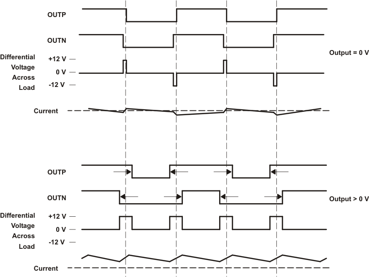
The TPA3111D1 uses a modulation scheme that allows operation without the classic LC reconstruction filter when the amp is driving an inductive load. Each output is switching from 0 V to the supply voltage. The OUTP and OUTN are in phase with each other with no input so that there is little or no current in the speaker. The duty cycle of OUTP is greater than 50% and OUTN is less than 50% for positive output voltages. The duty cycle of OUTP is less than 50% and OUTN is greater than 50% for negative output voltages. The voltage across the load sits at 0 V throughout most of the switching period, greatly reducing the switching current, which reduces any I2R losses in the load.
 Figure 16. The TPA3111D1 Output Voltage and Current Waveforms into an Inductive Load