SLOS938F May   2016  – January 2020 TPA3136AD2 , TPA3136D2

PRODUCTION DATA.  

  1. Features
  2. Applications
  3. Description
    1.     Device Images
      1.      Simplified Schematic
  4. Revision History
  5. Device Comparison Table
  6. Pin Configuration and Functions
    1.     Pin Functions
  7. Specifications
    1. 7.1 Absolute Maximum Ratings
    2. 7.2 ESD Ratings
    3. 7.3 Recommended Operating Conditions
    4. 7.4 Thermal Information
    5. 7.5 Electrical Characteristics
    6. 7.6 Switching Characteristics
    7. 7.7 Typical Characteristics
  8. Parameter Measurement Information
  9. Detailed Description
    1. 9.1 Overview
    2. 9.2 Functional Block Diagram
    3. 9.3 Feature Description
      1. 9.3.1 Fixed Analog Gain
      2. 9.3.2 SD Operation
      3. 9.3.3 PLIMIT
      4. 9.3.4 Spread Spectrum and De-Phase Control
      5. 9.3.5 GVDD Supply
      6. 9.3.6 DC Detect
      7. 9.3.7 PBTL Select
      8. 9.3.8 Short-Circuit Protection and Automatic Recovery Feature
      9. 9.3.9 Thermal Protection
    4. 9.4 Device Functional Modes
  10. 10Application and Implementation
    1. 10.1 Application Information
    2. 10.2 Typical Applications
      1. 10.2.1 Design Requirements
        1. 10.2.1.1 PCB Material Recommendation
        2. 10.2.1.2 PVCC Capacitor Recommendation
        3. 10.2.1.3 Decoupling Capacitor Recommendations
      2. 10.2.2 Detailed Design Procedure
        1. 10.2.2.1 Ferrite Bead Filter Considerations
        2. 10.2.2.2 Efficiency: LC Filter Required with the Traditional Class-D Modulation Scheme
        3. 10.2.2.3 When to Use an Output Filter for EMI Suppression
        4. 10.2.2.4 Input Resistance
        5. 10.2.2.5 Input Capacitor, Ci
        6. 10.2.2.6 BSN and BSP Capacitors
        7. 10.2.2.7 Differential Inputs
        8. 10.2.2.8 Using Low-ESR Capacitors
      3. 10.2.3 Application Performance Curves
        1. 10.2.3.1 EN55013 Radiated Emissions Results
        2. 10.2.3.2 EN55022 Conducted Emissions Results
  11. 11Power Supply Recommendations
    1. 11.1 Power Supply Decoupling, CS
  12. 12Layout
    1. 12.1 Layout Guidelines
    2. 12.2 Layout Example
  13. 13Device and Documentation Support
    1. 13.1 Device Support
      1. 13.1.1 Third-Party Products Disclaimer
    2. 13.2 Documentation Support
      1. 13.2.1 Related Documentation
    3. 13.3 Related Links
    4. 13.4 Receiving Notification of Documentation Updates
    5. 13.5 Support Resources
    6. 13.6 Trademarks
    7. 13.7 Electrostatic Discharge Caution
    8. 13.8 Glossary
  14. 14Mechanical, Packaging, and Orderable Information

Package Options

Mechanical Data (Package|Pins)
Thermal pad, mechanical data (Package|Pins)
Orderable Information

Typical Applications

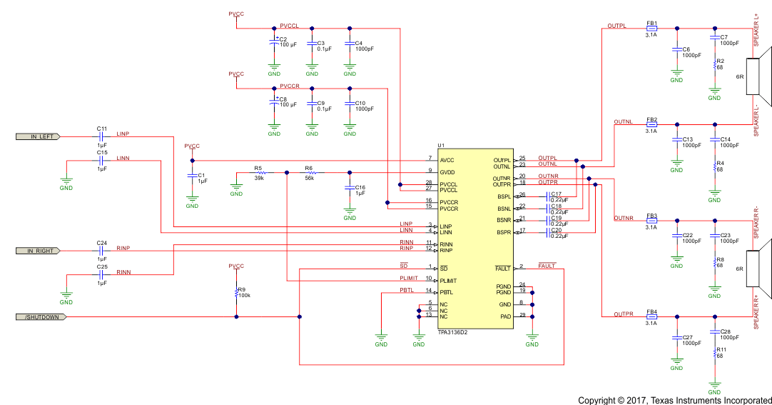
TPA3136D2 TPA3136AD2 TPA3136D2_TypAppSchBTL.gif
Figure 18. Stereo Class-D Amplifier with BTL Output and Single-Ended Inputs with Spread Spectrum Modulation

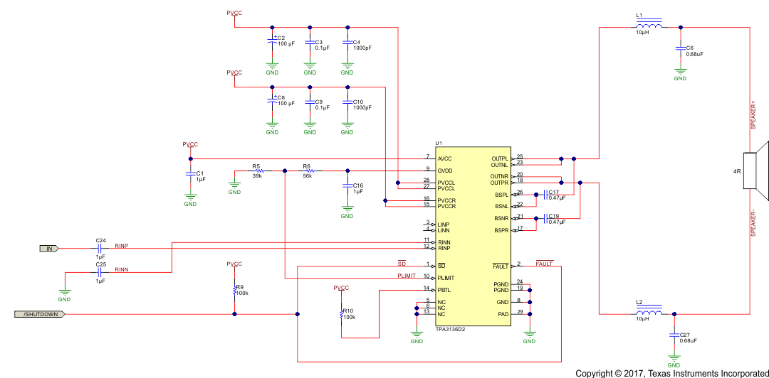
TPA3136D2 TPA3136AD2 TPA3136D2_TypAppPBTL.gifFigure 19. Stereo Class-D Amplifier with PBTL Output and Single-Ended Input with Spread Spectrum Modulation