SLASEC7A September 2016 – October 2016 TPA3245
PRODUCTION DATA.
- 1 Features
- 2 Applications
- 3 Description
- 4 Revision History
- 5 Device Comparison Table
- 6 Pin Configuration and Functions
-
7 Specifications
- 7.1 Absolute Maximum Ratings
- 7.2 ESD Ratings
- 7.3 Recommended Operating Conditions
- 7.4 Thermal Information
- 7.5 Electrical Characteristics
- 7.6 Audio Characteristics (BTL)
- 7.7 Audio Characteristics (SE)
- 7.8 Audio Characteristics (PBTL)
- 7.9 Typical Characteristics, BTL Configuration
- 7.10 Typical Characteristics, SE Configuration
- 7.11 Typical Characteristics, PBTL Configuration
- 8 Parameter Measurement Information
-
9 Detailed Description
- 9.1 Overview
- 9.2 Functional Block Diagrams
- 9.3 Feature Description
- 9.4
Device Protection System
- 9.4.1 Overload and Short Circuit Current Protection
- 9.4.2 Signal Clipping and Pulse Injector
- 9.4.3 DC Speaker Protection
- 9.4.4 Pin-to-Pin Short Circuit Protection (PPSC)
- 9.4.5 Overtemperature Protection OTW and OTE
- 9.4.6 Undervoltage Protection (UVP) and Power-on Reset (POR)
- 9.4.7 Fault Handling
- 9.4.8 Device Reset
-
10Application and Implementation
- 10.1 Application Information
- 10.2 Typical Applications
- 11Power Supply Recommendations
-
12Layout
- 12.1 Layout Guidelines
- 12.2
Layout Examples
- 12.2.1 BTL Application Printed Circuit Board Layout Example
- 12.2.2 SE Application Printed Circuit Board Layout Example
- 12.2.3 PBTL (Outputs Paralleled before LC filter) Application Printed Circuit Board Layout Example
- 12.2.4 PBTL (Outputs Paralleled after LC filter) Application Printed Circuit Board Layout Example
- 13Device and Documentation Support
- 14Mechanical, Packaging, and Orderable Information
Package Options
Mechanical Data (Package|Pins)
- DDV|44
Thermal pad, mechanical data (Package|Pins)
- DDV|44
Orderable Information
10 Application and Implementation
NOTE
Information in the following applications sections is not part of the TI component specification, and TI does not warrant its accuracy or completeness. TI’s customers are responsible for determining suitability of components for their purposes. Customers should validate and test their design implementation to confirm system functionality.
10.1 Application Information
TPA3245 can be configured either in stereo BTL mode, 4 channel SE mode, mono PBTL mode, or in 2.1 mixed 1x BTL + 2x SE mode depending on output power conditions and system design.
10.2 Typical Applications
10.2.1 Stereo BTL Application
This section provides an example for configuring the TPA3245 in bridge-tied load (BTL) mode.
 Figure 26. Typical Differential (2N) BTL Application
10.2.1.1 Design Requirements
For this design example, use the parameters in Table 6.
Table 6. Design Requirements, BTL Application
| DESIGN PARAMETER | EXAMPLE |
|---|---|
| Low Power (Pull-up) Supply | 3.3 V |
| Mid Power Supply 12 V | 12 V |
| High Power Supply | 12 - 30 V |
| Mode Selection | M2 = L |
| M1 = L | |
| Analog Inputs | INPUT_A = ±3.9 V (peak, max) |
| INPUT_B = ± 3.9V (peak, max) | |
| INPUT_C = ±3.9 V (peak, max) | |
| INPUT_D = ±3.9 V (peak, max) | |
| Output Filters | Inductor-Capacitor Low Pass FIlter (10 µH + 1 µF) |
| Speaker Impedance | 3-8 Ω |
10.2.1.2 Detailed Design Procedures
A rising-edge transition on reset input allows the device to execute the startup sequence and starts switching.
The CLIP signal is indicating that the output is approaching clipping. The signal can be used either to decrease audio volume or to control an intelligent power supply nominally operating at a low rail adjusting to a higher supply rail.
The device is inverting the audio signal from input to output.
The DVDD and AVDD pins are not recommended to be used as a voltage sources for external circuitry.
10.2.1.2.1 Decoupling Capacitor Recommendations
In order to design an amplifier that has robust performance, passes regulatory requirements, and exhibits good audio performance, good quality decoupling capacitors should be used. In practice, X7R should be used in this application.
10.2.1.2.2 PVDD Capacitor Recommendation
The PVDD decoupling capacitors must be placed as close to the device pins a possible to insure short trace length and low a low inductance path. Likewise the ground path for these capacitors must provide a good reference and should be substantial. This will keep voltage ringing on PVDD to a minimum.
The voltage of the decoupling capacitors should be selected in accordance with good design practices. Temperature, ripple current, and voltage overshoot must be considered. This fact is particularly true in the selection of the 1μF that is placed on the power supply to each full-bridge. It must withstand the voltage overshoot of the PWM switching, the heat generated by the amplifier during high power output, and the ripple current created by high power output. A minimum voltage rating of 50 V is required for use with a 30V power supply.
The large capacitors used in conjunction with each full-bridge, are referred to as the PVDD Capacitors. These capacitors should be selected for proper voltage margin and adequate capacitance to support the power requirements. In practice, with a well designed system power supply, 1000 μF, 50 V supports most applications. The PVDD capacitors should be low ESR type because they are used in a circuit associated with high-speed switching.
10.2.1.2.3 PCB Material Recommendation
FR-4 Glass Epoxy material with 2 oz. (70 μm) copper is recommended for use with the TPA3245. The use of this material can provide for higher power output, improved thermal performance, and better EMI margin (due to lower PCB trace inductance.
10.2.1.2.4 Oscillator
The built in oscillator frequency can be trimmed by an external resistor from the FREQ_ADJ pin to GND. Changes in the oscillator frequency should be made with resistor values specified in Recommended Operating Conditions while RESET is low.
To reduce interference problems while using a radio receiver tuned within the AM band, the switching frequency can be changed from nominal to lower or higher values. These values should be chosen such that the nominal and the alternate switching frequencies together result in the fewest cases of interference throughout the AM band. The oscillator frequency can be selected by the value of the FREQ_ADJ resistor connected to GND in master mode.
For slave mode operation, turn off the oscillator by pulling the FREQ_ADJ pin to DVDD. This configures the OSC_I/O pins as inputs to be slaved from an external differential clock. In a master/slave system inter-channel delay is automatically set up between the switching of the audio channels, which can be illustrated by no idle channels switching at the same time. This will not influence the audio output, but only the switch timing to minimize noise coupling between audio channels through the power supply. Inter-channel delay is needed to optimize audio performance and to get better operating conditions for the power supply. The inter-channel delay will be set up for a slave device depending on the polarity of the OSC_I/O connection as follows:
- Slave 1 mode has normal polarity (master + to slave + and master - to slave -)
- Slave 2 mode has reverse polarity (master + to slave - and master - to slave +)
The interchannel delay for interleaved channel idle switching is given in the table below for the master/slave and output configuration modes in degrees relative to the PWM frame.
Table 7. Master/Slave Inter Channel Delay Settings
| Master | M1 = 0, M2 = 0, 2 x BTL mode | M1 = 1, M2 = 0, 1 x BTL + 2 x SE mode | M1 = 0, M2 = 1, 1 x PBTL mode | M1 = 1, M2 = 1, 4 x SE mode |
|---|---|---|---|---|
| OUT_A | 0° | 0° | 0° | 0° |
| OUT_B | 180° | 180° | 180° | 60° |
| OUT_C | 60° | 60° | 0° | 0° |
| OUT_D | 240° | 120° | 180° | 60° |
| Slave 1 | ||||
| OUT_A | 60° | 60° | 60° | 60° |
| OUT_B | 240° | 240° | 240° | 120° |
| OUT_C | 120° | 120° | 60° | 60° |
| OUT_D | 300° | 180° | 240° | 120° |
| Slave 2 | ||||
| OUT_A | 30° | 30° | 30° | 30° |
| OUT_B | 210° | 210° | 210° | 90° |
| OUT_C | 90° | 90° | 30° | 30° |
| OUT_D | 270° | 150° | 210° | 90° |
10.2.2 Application Curves
Relevant performance plots for TPA3245 in BTL configuration are shown in Typical Characteristics, BTL Configuration
Table 8. Relevant Performance Plots, BTL Configuration
| PLOT TITLE | FIGURE NUMBER |
|---|---|
| Total Harmonic Distortion+Noise vs Frequency | Figure 1 |
| Total Harmonic Distortion+Noise vs Frequency, 80kHz analyzer BW | Figure 2 |
| Total Harmonic Distortion + Noise vs Output Power | Figure 3 |
| Output Power vs Supply Voltage, 10% THD+N | Figure 4 |
| Output Power vs Supply Voltage, 10% THD+N | Figure 6 |
| System Efficiency vs Output Power | Figure 6 |
| System Power Loss vs Output Power | Figure 7 |
| Output Power vs Case Temperature | Figure 8 |
| Noise Amplitude vs Frequency | Figure 9 |
10.2.3 Typical Application, Single Ended (1N) SE
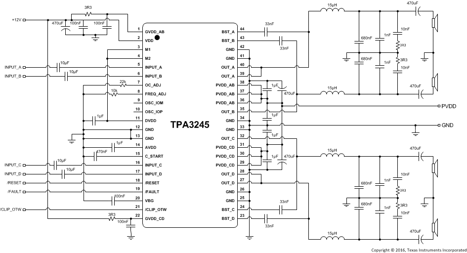
This section provides an example for configuring the TPA3245 in single-ended output (SE) mode.
 Figure 27. Typical Single Ended (1N) SE Application
10.2.3.1 Design Requirements
Refer to Stereo BTL Application for the Design Requirements.
Table 9. Design Requirements, SE Application
| DESIGN PARAMETER | EXAMPLE |
|---|---|
| Low Power (Pull-up) Supply | 3.3 V |
| Mid Power Supply 1 2V | 12 V |
| High Power Supply | 12 - 30 V |
| Mode Selection | M2 = H |
| M1 = H | |
| Analog Inputs | INPUT_A = ±3.9 V (peak, max) |
| INPUT_B = ±3.9 V (peak, max) | |
| INPUT_C = ±3.9 V (peak, max) | |
| INPUT_D = ±3.9 V (peak, max) | |
| Output Filters | Inductor-Capacitor Low Pass FIlter (15 µH + 680 nF) |
| Speaker Impedance | 2 - 8 Ω |
10.2.3.2 Detailed Design Procedures
Refer to Stereo BTL Application for the Detailed Design Procedures.
10.2.3.3 Application Curves
Relevant performance plots for TPA3245 in SE configuration are shown in Typical Characteristics, SE Configuration
Table 10. Relevant Performance Plots, SE Configuration
| PLOT TITLE | FIGURE NUMBER |
|---|---|
| Total Harmonic Distortion+Noise vs Output Power | Figure 10 |
| Total Harmonic Distortion+Noise vs Frequency | Figure 11 |
| Total Harmonic Distortion+Noise vs Frequency, 80kHz analyzer BW | Figure 12 |
| Output Power vs Supply Voltage, 10% THD+N | Figure 13 |
| Output Power vs Supply Voltage, 1% THD+N | Figure 14 |
| Output Power vs Case Temperature | Figure 15 |
10.2.4 Typical Application, Differential (2N), PBTL (Outputs Paralleled before LC filter)
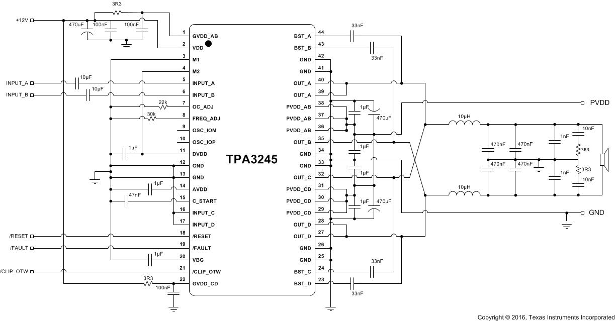
TPA3245 can be configured in mono PBTL mode by paralleling the outputs before the LC filter or after the LC filter (seeTypical Application, Differential (2N), PBTL (Outputs Paralleled after LC filter)). Paralleled outputs before the LC filter is recommended for better performance and limiting the number of output LC filter inductors, only two inductors required. This sections shows an example of paralleled outputs before the LC filter.
 Figure 28. Typical Differential (2N) PBTL (Outputs Paralleled before LC filter) Application
10.2.4.1 Design Requirements
Refer to Stereo BTL Application for the Design Requirements.
Table 11. Design Requirements, PBTL (Outputs Paralleled before LC filter) Application
| DESIGN PARAMETER | EXAMPLE |
|---|---|
| Low Power (Pull-up) Supply | 3.3 V |
| Mid Power Supply 12 V | 12 V |
| High Power Supply | 12 - 30 V |
| Mode Selection | M2 = H |
| M1 = L | |
| Analog Inputs | INPUT_A = ±3.9V (peak, max) |
| INPUT_B = ±3.9V (peak, max) | |
| INPUT_C = Grounded | |
| INPUT_D = Grounded | |
| Output Filters | Inductor-Capacitor Low Pass FIlter (10 µH + 1 µF) |
| Speaker Impedance | 2 - 4 Ω |
10.2.4.2 Detailed Design Procedures
Refer to Stereo BTL Application for the Detailed Design Procedures.
10.2.4.3 Application Curves
Relevant performance plots for TPA3245 in PBTL configuration are shown in Typical Characteristics, PBTL Configuration
Table 12. Relevant Performance Plots, PBTL (Outputs Paralleled before LC filter) Configuration
| PLOT TITLE | FIGURE NUMBER |
|---|---|
| Total Harmonic Distortion+Noise vs Output Power | Figure 16 |
| Total Harmonic Distortion+Noise vs Frequency | Figure 17 |
| Total Harmonic Distortion+Noise vs Frequency, 80kHz analyzer BW | Figure 18 |
| Output Power vs Supply Voltage, 10% THD+N | Figure 19 |
| Output Power vs Supply Voltage, 1% THD+N | Figure 20 |
| Output Power vs Case Temperature | Figure 21 |
10.2.5 Typical Application, Differential (2N), PBTL (Outputs Paralleled after LC filter)
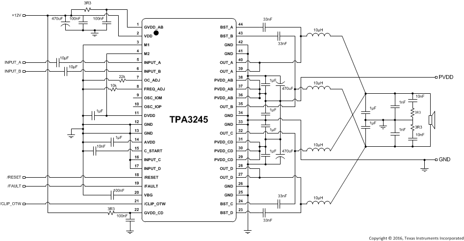
TPA3245 can be configured in mono PBTL mode by paralleling the outputs before the LC filter (see Typical Application, Differential (2N), PBTL (Outputs Paralleled before LC filter)) or after the LC filter. Paralleled outputs after the LC filter may be preferred if: a single board design must support both PBTL and BTL, or in the case multiple, smaller paralleled inductors are preferred due to size or cost. Paralleling after the LC filter requires four inductors, one for each OUT_x. This section shows an example of paralleled outputs after the LC filter.
 Figure 29. Typical Differential (2N) PBTL (Outputs Paralleled after LC filter) Application
10.2.5.1 Design Requirements
Refer to Stereo BTL Application for the Design Requirements.
Table 13. Design Requirements, PBTL (Outputs Paralleled after LC filter) Application
| DESIGN PARAMETER | EXAMPLE |
|---|---|
| Low Power (Pull-up) Supply | 3.3 V |
| Mid Power Supply 12 V | 12 V |
| High Power Supply | 12 - 30 V |
| Mode Selection | M2 = H |
| M1 = L | |
| Analog Inputs | INPUT_A = ±3.9V (peak, max) |
| INPUT_B = ±3.9V (peak, max) | |
| INPUT_C = Grounded | |
| INPUT_D = Grounded | |
| Output Filters | Inductor-Capacitor Low Pass FIlter (10 µH + 1 µF) |
| Speaker Impedance | 2 - 4 Ω |
10.2.5.2 Detailed Design Procedures
Refer to Stereo BTL Application for the Detailed Design Procedures.