SLOS313C December 2000 – March 2016 TPA6111A2
PRODUCTION DATA.
- 1 Features
- 2 Applications
- 3 Description
- 4 Revision History
- 5 Device Comparison Table
- 6 Pin Configuration and Functions
-
7 Specifications
- 7.1 Absolute Maximum Ratings
- 7.2 ESD Ratings
- 7.3 Recommended Operating Conditions
- 7.4 Thermal Information
- 7.5 DC Electrical Characteristics, VDD = 3.3 V
- 7.6 AC Operating Characteristics, VDD = 3.3 V
- 7.7 DC Electrical Characteristics, VDD = 5.5 V
- 7.8 AC Operating Characteristics, VDD = 5.5 V
- 7.9 AC Operating Characteristics, VDD = 3.3 V
- 7.10 AC Operating Characteristics, VDD = 5 V
- 7.11 Typical Characteristics
- 8 Parameter Measurement Information
- 9 Detailed Description
- 10Application and Implementation
- 11Power Supply Recommendations
- 12Layout
- 13Device and Documentation Support
- 14Mechanical, Packaging, and Orderable Information
Package Options
Refer to the PDF data sheet for device specific package drawings
Mechanical Data (Package|Pins)
- D|8
- DGN|8
Thermal pad, mechanical data (Package|Pins)
- DGN|8
Orderable Information
1 Features
2 Applications
- Smart Phones and Wireless Handsets
- Portable Tablets
- Notebook PCs and Docking Stations
3 Description
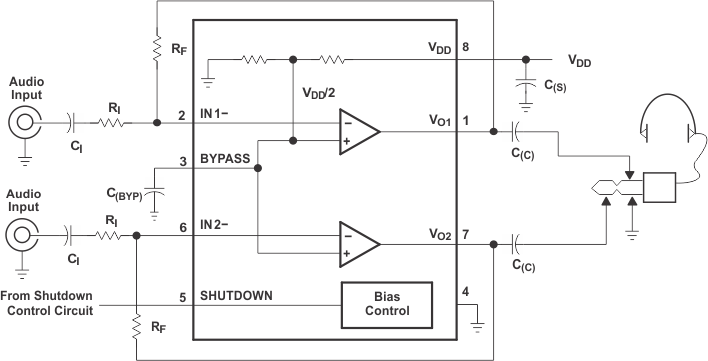
The TPA6111A2 is a stereo audio power amplifier packaged in either an 8-pin SOIC or an 8-pin PowerPAD MSOP package capable of delivering 150 mW of continuous RMS power per channel into 16-Ω loads. Amplifier gain is externally configured by means of two resistors per input channel and does not require external compensation for settings of 0 to 20 dB.
THD+N, when driving a 16-Ω load from 5 V, is 0.03% at 1 kHz, and less than 1% across the audio band of 20 Hz to 20 kHz. For 32-Ω loads, the THD+N is reduced to less than 0.02% at 1 kHz, and is less than 1% across the audio band of 20 Hz to 20 kHz. For 10-kΩ loads, the THD+N performance is 0.005% at 1 kHz, and less than 0.5% across the audio band of 20 Hz to 20 kHz.
Device Information(1)
| PART NUMBER | PACKAGE | BODY SIZE (NOM) |
|---|---|---|
| TPA6111A2 | SOIC (8) | 4.90 mm × 3.91 mm |
| MSOP (8) | 3.00 mm × 3.00 mm |
- For all available packages, see the orderable addendum at the end of the data sheet.
Typical Application Circuit
