SLOS313C December 2000 – March 2016 TPA6111A2
PRODUCTION DATA.
- 1 Features
- 2 Applications
- 3 Description
- 4 Revision History
- 5 Device Comparison Table
- 6 Pin Configuration and Functions
-
7 Specifications
- 7.1 Absolute Maximum Ratings
- 7.2 ESD Ratings
- 7.3 Recommended Operating Conditions
- 7.4 Thermal Information
- 7.5 DC Electrical Characteristics, VDD = 3.3 V
- 7.6 AC Operating Characteristics, VDD = 3.3 V
- 7.7 DC Electrical Characteristics, VDD = 5.5 V
- 7.8 AC Operating Characteristics, VDD = 5.5 V
- 7.9 AC Operating Characteristics, VDD = 3.3 V
- 7.10 AC Operating Characteristics, VDD = 5 V
- 7.11 Typical Characteristics
- 8 Parameter Measurement Information
- 9 Detailed Description
- 10Application and Implementation
- 11Power Supply Recommendations
- 12Layout
- 13Device and Documentation Support
- 14Mechanical, Packaging, and Orderable Information
Package Options
Refer to the PDF data sheet for device specific package drawings
Mechanical Data (Package|Pins)
- D|8
- DGN|8
Thermal pad, mechanical data (Package|Pins)
- DGN|8
Orderable Information
9 Detailed Description
9.1 Overview
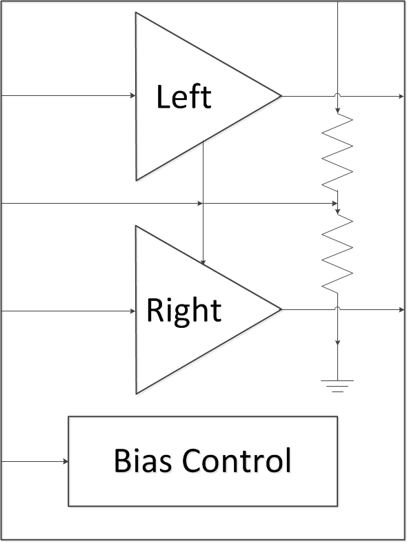
The TPA6111A2 device is a stereo audio power amplifier available in 8-pin SOIC and 8-pin MSOP packages. This device is able to deliver 150 mW of continuous RMS power per channel into 16-Ω loads. The gain of the amplifier is externally configured from 0 dB to 20 dB through two resistors per channel. The TPA6111A2 device is fully specified for operation at 3.3 V and 5 V, which makes this device ideal for PC and mobile applications.
9.2 Functional Block Diagram

9.3 Feature Description
9.3.1 5-V Versus 3.3-V Operation
The TPA6111A2 was designed for operation over a supply range of 2.5 V to 5.5 V. This data sheet provides full specifications for 5-V and 3.3-V operation because these are considered to be the two most common standard voltages. There are no special considerations for 3.3-V versus 5-V operation as far as supply bypassing, gain setting, or stability. The most important consideration is that of output power. Each amplifier in the TPA6111A2 can produce a maximum voltage swing of VDD – 1 V. This means, for 3.3-V operation, clipping starts to occur when VO(PP) = 2.3 V as opposed when VO(PP) = 4 V while operating at 5 V. The reduced voltage swing subsequently reduces maximum output power into the load before distortion begins to become significant.
9.4 Device Functional Modes
The TPA6111A2 can be put in shutdown mode when asserting SHUTDOWN pin to a logic HIGH level. While in shutdown mode, the device is turned off, making the current consumption very low. The device exits shutdown mode when a LOW logic level is applied to SHUTDOWN pin.