SLOS490C July 2006 – November 2015
PRODUCTION DATA.
- 1 Features
- 2 Applications
- 3 Description
- 4 Revision History
- 5 Device Comparison Table
- 6 Pin Configuration and Functions
- 7 Specifications
- 8 Parameter Measurement Information
- 9 Detailed Description
- 10Application and Implementation
- 11Power Supply Recommendations
- 12Layout
- 13Device and Documentation Support
- 14Mechanical, Packaging, and Orderable Information
Package Options
Mechanical Data (Package|Pins)
Thermal pad, mechanical data (Package|Pins)
Orderable Information
1 Features
- 1.25 W Into 8-Ω From a 5-V Supply at THD = 1% (Typical)
- Shutdown Pin has 1.8-V Compatible Thresholds
- Low Supply Current: 1.7 mA Typical
- Shutdown Current < 10 µA
- Only Five External Components
- Improved PSRR (90 dB) and Wide Supply Voltage (2.5 V to 5.5 V) for Direct Battery Operation
- Fully Differential Design Reduces RF Rectification
- Improved CMRR Eliminates Two Input Coupling Capacitors
- C(BYPASS) Is Optional Due to Fully Differential Design and High PSRR
- Available in 3-mm × 3-mm QFN Package (DRB)
- Available in an 8-Pin PowerPAD™ MSOP (DGN)
- Available in a 2-mm × 2-mm MicroStar Junior™ BGA Package (ZQV)
2 Applications
- Designed for Wireless Handsets, PDAs, and Other Mobile Devices
- Compatible With Low Power (1.8-V Logic) I/O Threshold Control Signals
3 Description
The TPA6205A1 device is a 1.25-W mono fully differential amplifier designed to drive a speaker with at least 8-Ω impedance while consuming less than 37 mm2 (ZQV package option) total printed-circuit-board (PCB) area in most applications. This device operates from 2.5 V to 5.5 V, drawing only 1.7 mA of quiescent supply current. The TPA6205A1 is available in the space-saving 2-mm × 2-mm MicroStar Junior BGA package, and the space saving 3-mm × 3-mm QFN (DRB) package.
Features like 85-dB PSRR from 90 Hz to 5 kHz, improved RF-rectification immunity, and small PCB area makes the TPA6205A1 ideal for wireless handsets. A fast start-up time of 4s with minimal pop makes the TPA6205A1 ideal for PDA applications.
Device Information(1)
| PART NUMBER | PACKAGE | BODY SIZE (NOM) |
|---|---|---|
| TPA6205A1 | MSOP-PowerPAD (8) | 3.00 mm × 3.00 mm |
| SON (8) | 3.00 mm × 3.00 mm | |
| BGA MICROSTAR JUNIOR (8) | 2.00 mm × 2.00 mm |
- For all available packages, see the orderable addendum at the end of the data sheet.
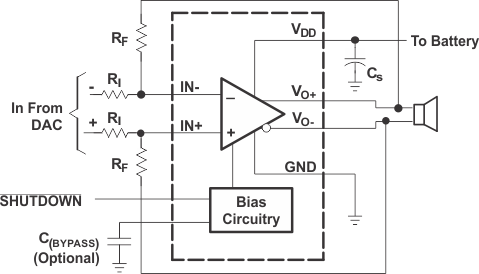
Application Circuit

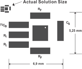
Example Solution Size
