SLOS490C July 2006 – November 2015
PRODUCTION DATA.
- 1 Features
- 2 Applications
- 3 Description
- 4 Revision History
- 5 Device Comparison Table
- 6 Pin Configuration and Functions
- 7 Specifications
- 8 Parameter Measurement Information
- 9 Detailed Description
- 10Application and Implementation
- 11Power Supply Recommendations
- 12Layout
- 13Device and Documentation Support
- 14Mechanical, Packaging, and Orderable Information
Package Options
Mechanical Data (Package|Pins)
Thermal pad, mechanical data (Package|Pins)
Orderable Information
10 Application and Implementation
NOTE
Information in the following applications sections is not part of the TI component specification, and TI does not warrant its accuracy or completeness. TI’s customers are responsible for determining suitability of components for their purposes. Customers should validate and test their design implementation to confirm system functionality.
10.1 Application Information
These typical connection diagrams highlight the required external components and system level connections for proper operation of the device in several popular cases. Each of these configurations can be realized using the Evaluation Modules (EVMs) for the device. These flexible modules allow full evaluation of the device in the most common modes of operation. Any design variation can be supported by TI through schematic and layout reviews. Visit http://e2e.ti.com for design assistance and join the audio amplifier discussion forum for additional information.
10.2 Typical Applications
Figure 32 through Figure 31 show application schematics for differential and single-ended inputs.
10.2.1 TPA6205A1 With Differential Input
The TPA6205A1 can be used with differential input without input capacitors. This section describes the design considerations for this application.
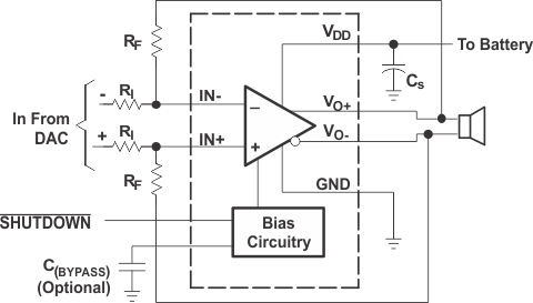 Figure 32. Typical Differential Input Application Schematic
10.2.1.1 Design Requirements
Table 3 lists the design parameters of the device.
Table 3. Design Parameters
| PARAMETER | EXAMPLE VALUE | |||
|---|---|---|---|---|
| Power Supply | 5 V | |||
| Shutdown Input | High > 2 V | |||
| Low < 0.8 V | ||||
| Speaker | 8 Ω | |||
10.2.1.2 Detailed Design Procedure
10.2.1.2.1 Selecting Components
Typical values are shown in Table 4.
Table 4. Typical Component Values
| COMPONENT | VALUE | |||
|---|---|---|---|---|
| RI | 10 kΩ | |||
| RF | 10 kΩ | |||
| C(BYPASS)(1) | 0.22 µF | |||
| CS | 1 µF | |||
| CI | 0.22 µF | |||
10.2.1.2.1.1 Resistors (RF and RI)
The input (RI) and feedback resistors (RF) set the gain of the amplifier according to Equation 23.

RF and RI should range from 1 kΩ to 100 kΩ. Most graphs were taken with RF = RI = 20 kΩ.
Resistor matching is very important in fully differential amplifiers. The balance of the output on the reference voltage depends on matched ratios of the resistors. CMRR, PSRR, and the cancellation of the second harmonic distortion diminishes if resistor mismatch occurs. Therefore, it is recommended to use 1% tolerance resistors or better to keep the performance optimized.
10.2.1.2.1.2 Bypass Capacitor (CBYPASS) and Start-Up Time
The internal voltage divider at the BYPASS pin of this device sets a mid-supply voltage for internal references and sets the output common mode voltage to VDD/2. Adding a capacitor to this pin filters any noise into this pin and increases the kSVR. C(BYPASS)also determines the rise time of VO+ and VO– when the device is taken out of shutdown. The larger the capacitor, the slower the rise time. Although the output rise time depends on the bypass capacitor value, the device passes audio 4 μs after taken out of shutdown and the gain is slowly ramped up based on C(BYPASS).
To minimize pops and clicks, design the circuit so the impedance (resistance and capacitance) detected by both inputs, IN+ and IN–, is equal.
10.2.1.2.1.3 Input Capacitor (CI)
The TPA6205A1 does not require input coupling capacitors if using a differential input source that is biased from 0.5 V to VDD – 0.8 V. Use 1% tolerance or better gain-setting resistors if not using input coupling capacitors.
In the single-ended input application an input capacitor, CI, is required to allow the amplifier to bias the input signal to the proper DC level. In this case, CI and RI form a high-pass filter with the corner frequency determined in Equation 24.

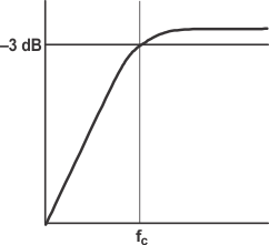 Figure 33. CI and RI High-Pass Filter Cutoff Frequency
The value of CI is important to consider as it directly affects the bass (low frequency) performance of the circuit. Consider the example where RI is 10 kΩ and the specification calls for a flat bass response down to 100 Hz. Equation 24 is reconfigured as Equation 25.

In this example, CI is 0.16 μF, so one would likely choose a value in the range of 0.22 μF to 0.47 μF. A further consideration for this capacitor is the leakage path from the input source through the input network
(RI , CI) and the feedback resistor (RF ) to the load. This leakage current creates a DC offset voltage at the input to the amplifier that reduces useful headroom, especially in high gain applications. For this reason, a ceramic capacitor is the best choice. When polarized capacitors are used, the positive side of the capacitor should face the amplifier input in most applications, as the dc level there is held at VDD/2, which is likely higher than the source dc level. It is important to confirm the capacitor polarity in the application.
10.2.1.2.1.4 Decoupling Capacitor (CS)
The TPA6205A1 is a high-performance CMOS audio amplifier that requires adequate power supply decoupling to ensure the output total harmonic distortion (THD) is as low as possible. Power supply decoupling also prevents oscillations for long lead lengths between the amplifier and the speaker. For higher frequency transients, spikes, or digital hash on the line, a good low equivalent-series-resistance (ESR) ceramic capacitor, typically 0.1 μF to 1 μF, placed as close as possible to the device VDD lead works best. For filtering lower frequency noise signals, a 10-μF or greater capacitor placed near the audio power amplifier also helps, but is not required in most applications because of the high PSRR of this device.
10.2.1.2.2 Using Low-ESR Capacitors
Low-ESR capacitors are recommended throughout this applications section. A real (as opposed to ideal) capacitor can be modeled simply as a resistor in series with an ideal capacitor. The voltage drop across this resistor minimizes the beneficial effects of the capacitor in the circuit. The lower the equivalent value of this resistance the more the real capacitor behaves like an ideal capacitor.
10.2.1.3 Application Curves
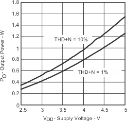
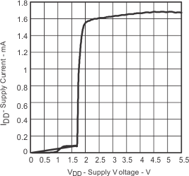
10.2.2 TPA6205A1 With Differential Input and Input Capacitors
The TPA6205A1 supports differential input operation with input capacitors. This section describes the design considerations for this application.
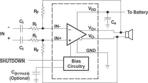 Figure 36. Differential Input Application Schematic Optimized With Input Capacitors
10.2.2.1 Design Requirements
Refer to the Design Requirements.
10.2.2.2 Detailed Design Procedure
Refer to the Detailed Design Procedure.
10.2.2.3 Application Curves
Refer to the Application Curves.
10.2.3 TPA6205A1 With Single-Ended Input
The TPA6205A1 can be used with single-ended inputs, using Input capacitors. This section describes the design considerations for this application.
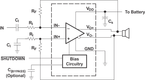 Figure 37. Single-Ended Input Application Schematic
10.2.3.1 Design Requirements
Refer to the Design Requirements.
10.2.3.2 Detailed Design Procedure
Refer to the Detailed Design Procedure.
10.2.3.3 Application Curves
Refer to the Application Curves.