SLOS367E August 2003 – November 2015 TPA6211A1
PRODUCTION DATA.
- 1 Features
- 2 Applications
- 3 Description
- 4 Revision History
- 5 Device Comparison Table
- 6 Pin Configuration and Functions
- 7 Specifications
- 8 Parameter Measurement Information
- 9 Detailed Description
-
10Application and Implementation
- 10.1 Application Information
- 10.2
Typical Application
- 10.2.1 Design Requirements
- 10.2.2 Detailed Design Procedure
- 10.2.3 Application Curves
- 10.3 System Examples
- 11Power Supply Recommendations
- 12Layout
- 13Device and Documentation Support
- 14Mechanical, Packaging, and Orderable Information
Package Options
Refer to the PDF data sheet for device specific package drawings
Mechanical Data (Package|Pins)
- DGN|8
- DRB|8
Thermal pad, mechanical data (Package|Pins)
Orderable Information
9 Detailed Description
9.1 Overview
The TPA6211A1 is a fully differential amplifier with differential inputs and outputs. The fully differential amplifier consists of a differential amplifier and a common- mode amplifier. The differential amplifier ensures that the amplifier outputs a differential voltage that is equal to the differential input times the gain. The common-mode feedback ensures that the common-mode voltage at the output is biased around VDD/2 regardless of the common- mode voltage at the input.
9.2 Functional Block Diagram
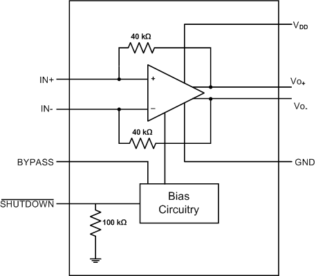
9.3 Feature Description
9.3.1 Fully Differential Amplifier Efficiency and Thermal Information
Class-AB amplifiers are inefficient, primarily because of voltage drop across the output-stage transistors. The two components of this internal voltage drop are the headroom or dc voltage drop that varies inversely to output power, and the sinewave nature of the output. The total voltage drop can be calculated by subtracting the RMS value of the output voltage from VDD. The internal voltage drop multiplied by the average value of the supply current, IDD(avg), determines the internal power dissipation of the amplifier.
An easy-to-use equation to calculate efficiency starts out as being equal to the ratio of power from the power supply to the power delivered to the load. To accurately calculate the RMS and average values of power in the load and in the amplifier, the current and voltage waveform shapes must first be understood (see Figure 28).
 Figure 28. Voltage and Current Waveforms for BTL Amplifiers
Although the voltages and currents for SE and BTL are sinusoidal in the load, currents from the supply are different between SE and BTL configurations. In an SE application the current waveform is a half-wave rectified shape, whereas in BTL it is a full-wave rectified waveform. This means RMS conversion factors are different. Keep in mind that for most of the waveform both the push and pull transistors are not on at the same time, which supports the fact that each amplifier in the BTL device only draws current from the supply for half the waveform. The following equations are the basis for calculating amplifier efficiency.
These definitions are true for the following equations:
- ηBTL = Efficiency of a BTL amplifier
- PL = Power delivered to load
- PSUP = Power drawn from power supply
- VLRMS = RMS voltage on BTL load
- VP = Peak voltage on BTL load
- VDD = Power supply voltage
- IDDavg = Average current drawn from the power supply
Use Equation 1 to calculate the efficiency of a BTL amplifier.

where
-

where
therefore
-
-

where
therefore
-
Using these values, substitute PL and PSUP from Equation 1 as shown in Equation 2.
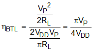
where
Therefore, ηBTL can be calculated using Equation 3.

Table 2. Efficiency and Maximum Ambient Temperature vs Output Power
| OUTPUT POWER (W) |
EFFICIENCY (%) |
INTERNAL DISSIPATION (W) |
POWER FROM SUPPLY (W) |
MAX AMBIENT TEMPERATURE (1)
(°C) |
|---|---|---|---|---|
| 5-V, 3-Ω Systems | ||||
| 0.5 | 27.2 | 1.34 | 1.84 | 85(2) |
| 1 | 38.4 | 1.6 | 2.6 | 76 |
| 2.45 | 60.2 | 1.62 | 4.07 | 75 |
| 3.1 | 67.7 | 1.48 | 4.58 | 82 |
| 5-V, 4-Ω BTL Systems | ||||
| 0.5 | 31.4 | 1.09 | 1.59 | 85(2) |
| 1 | 44.4 | 1.25 | 2.25 | 85(2) |
| 2 | 62.8 | 1.18 | 3.18 | 85(2) |
| 2.8 | 74.3 | 0.97 | 3.77 | 85(2) |
| 5-V, 8-Ω Systems | ||||
| 0.5 | 44.4 | 0.625 | 1.13 | 85(2) |
| 1 | 62.8 | 0.592 | 1.6 | 85(2) |
| 1.36 | 73.3 | 0.496 | 1.86 | 85(2) |
| 1.7 | 81.9 | 0.375 | 2.08 | 85(2) |
Table 2 uses Equation 3 to calculate efficiencies for four different output power levels. Note that the efficiency of the amplifier is quite low for lower power levels and rises sharply as power to the load is increased resulting in a nearly flat internal power dissipation over the normal operating range. Note that the internal dissipation at full output power is less than in the half power range. Calculating the efficiency for a specific system is the key to proper power supply design. For a 2.8-W audio system with 4-Ω loads and a 5-V supply, the maximum draw on the power supply is almost 3.8 W.
A final point to remember about Class-AB amplifiers is how to manipulate the terms in the efficiency equation to the utmost advantage when possible. Note that in Equation 3, VDD is in the denominator. This indicates that as VDD goes down, efficiency goes up.
Use Equation 4 as a simple formula for calculating the maximum power dissipated, PDmax, for a differential output application.

where
- PDmax for a 5-V, 4-Ω system is 1.27 W.
The maximum ambient temperature depends on the heat sinking ability of the PCB system. The derating factor for the 3 mm ×3 mm DRB package is shown in the dissipation rating table. Converting this to θJA:

Given θJA, the maximum allowable junction temperature, and the maximum internal dissipation, the maximum ambient temperature can be calculated with Equation 6. The maximum recommended junction temperature for the TPA6211A1 is 150°C.

Equation 6 shows that the maximum ambient temperature is 91.7°C (package limited to 85°C ambient) at maximum power dissipation with a 5-V supply.
Table 2 shows that for most applications no airflow is required to keep junction temperatures in the specified range. The TPA6211A1 is designed with thermal protection that turns the device off when the junction temperature surpasses 150°C to prevent damage to the IC. In addition, using speakers with an impedance higher than 4-Ω dramatically increases the thermal performance by reducing the output current.
9.3.1.1 Advantages of Fully Differential Amplifiers
- Input coupling capacitors not required: A fully differential amplifier with good CMRR, like the TPA6211A1, allows the inputs to be biased at voltage other than mid-supply. For example, if a DAC has a lower mid-supply voltage than that of the TPA6211A1, the common-mode feedback circuit compensates, and the outputs are still biased at the mid-supply point of the TPA6211A1. The inputs of the TPA6211A1 can be biased from 0.5 V to VDD - 0.8 V. If the inputs are biased outside of that range, input coupling capacitors are required.
- Mid-supply bypass capacitor, C(BYPASS), not required: The fully differential amplifier does not require a bypass capacitor. Any shift in the mid-supply voltage affects both positive and negative channels equally, thus canceling at the differential output. Removing the bypass capacitor slightly worsens power supply rejection ratio (kSVR), but a slight decrease of kSVR may be acceptable when an additional component can be eliminated (See Figure 17).
- Better RF-immunity: GSM handsets save power by turning on and shutting off the RF transmitter at a rate of 217 Hz. The transmitted signal is picked-up on input and output traces. The fully differential amplifier cancels the signal much better than the typical audio amplifier.
- Figure 31 through Figure 38 show application schematics for differential and single-ended inputs.
9.3.1.2 Differential Output Versus Single-Ended Output
Figure 29 shows a Class-AB audio power amplifier (APA) in a fully differential configuration. The TPA6211A1 amplifier has differential outputs driving both ends of the load. One of several potential benefits to this configuration is power to the load. The differential drive to the speaker means that as one side is slewing up, the other side is slewing down, and vice versa. This in effect doubles the voltage swing on the load as compared to a ground-referenced load. Plugging 2 × VO(PP) into the power equation, where voltage is squared, yields 4× the output power from the same supply rail and load impedance Equation 7.
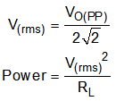
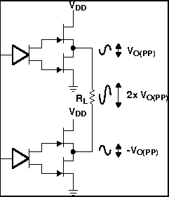 Figure 29. Differential Output Configuration
In a typical wireless handset operating at 3.6 V, bridging raises the power into an 8-Ω speaker from a singled-ended (SE, ground reference) limit of 200 mW to 800 mW. This is a 6-dB improvement in sound power—loudness that can be heard. In addition to increased power, there are frequency-response concerns. Consider the single-supply SE configuration shown in Figure 30. A coupling capacitor (CC) is required to block the dc-offset voltage from the load. This capacitor can be quite large (approximately 33 μF to 1000 μF) so it tends to be expensive, heavy, occupy valuable PCB area, and have the additional drawback of limiting low-frequency performance. This frequency-limiting effect is due to the high-pass filter network created with the speaker impedance and the coupling capacitance. This is calculated with Equation 8.

For example, a 68-μF capacitor with an 8-Ω speaker would attenuate low frequencies below 293 Hz. The BTL configuration cancels the dc offsets, which eliminates the need for the blocking capacitors. Low-frequency performance is then limited only by the input network and speaker response. Cost and PCB space are also minimized by eliminating the bulky coupling capacitor.
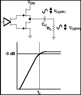 Figure 30. Single-Ended Output and Frequency Response
Increasing power to the load does carry a penalty of increased internal power dissipation. The increased dissipation is understandable considering that the BTL configuration produces 4× the output power of the SE configuration.
9.4 Device Functional Modes
9.4.1 Shutdown Mode
The TPA6211A1 device can be put in shutdown mode when asserting SHUTDOWN pin to a logic LOW. While in shutdown mode, the device output stage is turned off and set into high impedance, making the current consumption very low. The device exits shutdown mode when a HIGH logic level is applied to SHUTDOWN pin.


