SLVSDN8B august 2016 – september 2023 TPD1E10B09-Q1
PRODUCTION DATA
- 1
- 1 Features
- 2 Applications
- 3 Description
- 4 Revision History
- 5 Pin Configuration and Functions
- 6 Specifications
-
7 Detailed Description
- 7.1 Overview
- 7.2 Functional Block Diagram
- 7.3
Feature Description
- 7.3.1 AEC-Q101 Qualified
- 7.3.2 IEC 61000-4-2 ESD Protection
- 7.3.3 ISO 10605 ESD Protection
- 7.3.4 IEC 61000-4-5 Surge Protection
- 7.3.5 IO Capacitance
- 7.3.6 Dynamic Resistance
- 7.3.7 DC Breakdown Voltage
- 7.3.8 Ultra Low Leakage Current
- 7.3.9 Clamping Voltage
- 7.3.10 Industrial Temperature Range
- 7.3.11 Space-Saving Footprint
- 7.4 Device Functional Modes
- 8 Application and Implementation
- 9 Device and Documentation Support
- 10Mechanical, Packaging, and Orderable Information
Package Options
Mechanical Data (Package|Pins)
- DPY|2
Thermal pad, mechanical data (Package|Pins)
- DPY|2
Orderable Information
3 Description
The TPD1E10B09-Q1 device is a bidirectional electrostatic discharge (ESD) transient voltage suppression (TVS) diode in a small 0402 industry standard package. This TVS protection diode is convenient for component placement in space-saving applications and features low RDYN and high IEC rating. The TPD1E10B09-Q1 is rated to dissipate ESD strikes above the maximum level specified in the IEC 61000-4-2 international standard (Level 4) offering ±20-kV contact discharge and ±20-kV IEC air-gap protection. ESD voltages can easily reach 5-kV and during extreme conditions these voltages can be significantly higher, causing damages to many integrated circuits. For example, in a low humidity environment voltages can exceed 20-kV.
The low dynamic resistance (0.5 Ω) and low clamping voltage (13 V at 1-A IPP) allows for system level protection against transient events, providing robust protection on designs that are exposed to ESD events. This device also features a 10-pF IO capacitance making it an excellent choice for audio lines, push buttons, memory interfaces, or GPIOs.
This device is also available without automotive qualification: TPD1E10B09.
| PART NUMBER | PACKAGE(1) | PACKAGE SIZE(2) |
|---|---|---|
| TPD1E10B09-Q1 | DPY (X1SON, 2) | 1 mm × 0.6 mm |
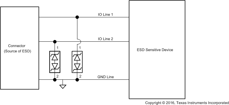
 Application Schematic