SLVSCP4B October 2014 – August 2015 TPD3S014 , TPD3S044
PRODUCTION DATA.
- 1 Features
- 2 Applications
- 3 Description
- 4 Revision History
- 5 Device Comparison Table
- 6 Pin Configuration and Functions
- 7 Specifications
- 8 Detailed Description
- 9 Application and Implementation
- 10Power Supply Recommendations
- 11Layout
- 12Device and Documentation Support
- 13Mechanical, Packaging, and Orderable Information
Package Options
Mechanical Data (Package|Pins)
- DBV|6
Thermal pad, mechanical data (Package|Pins)
Orderable Information
7 Specifications
7.1 Absolute Maximum Ratings
over operating free-air temperature (unless otherwise noted)(1)(2)| MIN | MAX | UNIT | ||
|---|---|---|---|---|
| Input voltage(3) | VIN | –0.3 | 6 | V |
| VOUT | –0.3 | 6 | ||
| EN | –0.3 | 6 | ||
| D1 | –0.3 | 6 | ||
| D2 | –0.3 | 6 | ||
| Voltage from VIN to VOUT | –6 | 6 | V | |
| Junction temperature, TJ | Internally limited | |||
| Storage temperature, Tstg | –65 | 150 | °C | |
(1) Stresses beyond those listed under Absolute Maximum Ratings may cause permanent damage to the device. These are stress ratings only, which do not imply functional operation of the device at these or any other conditions beyond those indicated under Recommended Operating Conditions. Exposure to absolute-maximum-rated conditions for extended periods may affect device reliability.
(2) Voltages are with respect to GND unless otherwise noted.
(3) See the Input and Output Capacitance section.
7.2 ESD Ratings
| VALUE | UNIT | |||||
|---|---|---|---|---|---|---|
| V(ESD) | Electrostatic discharge | Human body model (HBM), per ANSI/ESDA/JEDEC JS-001(1) | All pins | ±2000 | V | |
| Charged device model (CDM), per JEDEC specification JESD22-C101(2) | All pins | ±500 | ||||
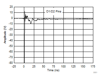
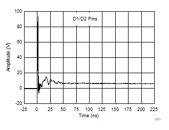
| IEC 61000-4-2 contact discharge(3) | VOUT, Dx pins | ±12000 | ||||
| IEC 61000-4-2 air-gap discharge(3) | VOUT, Dx pins | ±15000 | ||||
(1) JEDEC document JEP155 states that 500-V HBM allows safe manufacturing with a standard ESD control process. Pins listed as ±2000 V may actually have higher performance.
(2) JEDEC document JEP157 states that 250-V CDM allows safe manufacturing with a standard ESD control process. Pins listed as ±500 V may actually have higher performance.
(3) VOUT was tested on a PCB with input and output bypassing capacitors of 0.1 µF and 120 µF, respectively.
7.3 Recommended Operating Conditions
over operating free-air temperature range (unless otherwise noted)| MIN | NOM | MAX | UNIT | ||
|---|---|---|---|---|---|
| VIN | Input voltage | 4.5 | 5.5 | V | |
| VEN | Input voltage, EN | 0 | 5.5 | V | |
| VIH | High-level Input voltage, EN | 2 | V | ||
| VIL | Low-level Input voltage, EN | 0.7 | V | ||
| CIN | Input decoupling capacitance, IN to GND | 0.1 | µF | ||
| IOUT(1) | Continuous output current (TPD3S014) | 0.5 | A | ||
| Continuous output current (TPD3S044) | 1.5 | ||||
| TJ | Operating junction temperature | –40 | 125 | °C | |
(1) Package and current ratings may require an ambient temperature derating of 85°C
7.4 Thermal Information
| THERMAL METRIC(1)(2) | TPD3S0x4 | UNIT | |
|---|---|---|---|
| DBV (SOT-23) | |||
| 6 PINS | |||
| RθJA | Junction-to-ambient thermal resistance | 185.8 | °C/W |
| RθJC(top) | Junction-to-case (top) thermal resistance | 124.7 | °C/W |
| RθJB | Junction-to-board thermal resistance | 32.0 | °C/W |
| ψJT | Junction-to-top characterization parameter | 23.7 | °C/W |
| ψJB | Junction-to-board characterization parameter | 31.5 | °C/W |
| RθJC(bot) | Junction-to-case (bottom) thermal resistance | N/A | °C/W |
| RθJA(Custom) | See the Power Dissipation and Junction Temperature section | 120.3 | °C/W |
(1) For more information about traditional and new thermal metrics, see the Semiconductor and IC Package Thermal Metrics application report, SPRA953.
(2) See Device Comparison Table.
7.5 Electrical Characteristics: TJ = TA = 25°C
Unless otherwise noted: VIN = 5 V, VEN = VIN, IOUT = 0 A. See Device Comparison Table for the rated current of each part number. Parametrics over a wider operational range are shown in the second Electrical Characteristics: –40°C ≤ TJ ≤ 125°C table.| PARAMETER | TEST CONDITIONS(1) | MIN | TYP | MAX | UNIT | |
|---|---|---|---|---|---|---|
| POWER SWITCH | ||||||
| RDS(on) | Input – Output resistance | TPD3S014 | 97 | 110 | mΩ | |
| TPD3S014: –40°C ≤ (TJ, TA) ≤ 85°C | 96 | 130 | ||||
| TPD3S044 | 74 | 91 | ||||
| TPD3S044: –40°C ≤ (TJ, TA) ≤ 85°C | 74 | 106 | ||||
| CURRENT LIMIT | ||||||
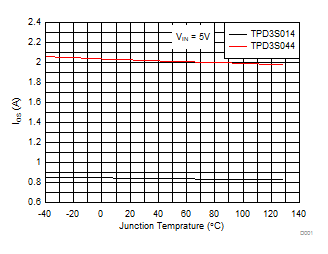
| IOS(2) | Current limit, see Figure 27 | TPD3S014 | 0.67 | 0.85 | 1.01 | A |
| TPD3S044 | 1.70 | 2.15 | 2.50 | |||
| SUPPLY CURRENT | ||||||
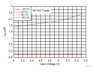
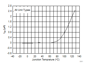
| ISD | Supply current, switch disabled | IOUT = 0A | 0.02 | 1 | µA | |
| –40°C ≤ (TJ, TA) ≤ 85°C, VIN = 5.5 V, IOUT = 0 A | 2 | |||||
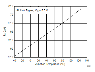
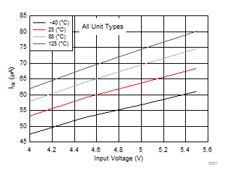
| ISE | Supply current, switch enabled | IOUT = 0A | 66 | 74 | µA | |
| –40°C ≤ (TJ, TA) ≤ 85°C, VIN = 5.5 V, IOUT = 0 A | 85 | |||||
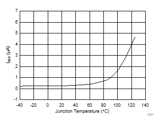
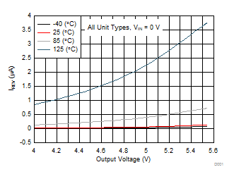
| IREV | Reverse leakage current | VOUT = 5 V, VIN = 0 V, Measure IVOUT | 0.2 | 1 | µA | |
| –40°C ≤ (TJ, TA) ≤ 85°C, VOUT = 5 V, VIN = 0 V, measure IVOUT | 5 | |||||
| OUTPUT DISCHARGE | ||||||
| RPD | Output pull-down resistance(3) | VIN = VOUT = 5 V, disabled | 400 | 456 | 600 | Ω |
| ESD PROTECTION | ||||||
| ΔCIO | Differential capacitance between the D1, D2 lines | ƒ = 1 MHz, VIO = 2.5 V | 0.02 | pF | ||
| CIO | (D1, D2 to GND) | ƒ = 1 MHz, VIO = 2.5 V | 1.4 | pF | ||
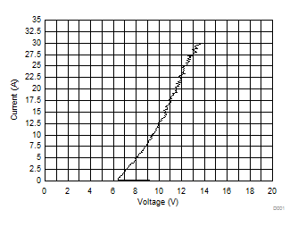
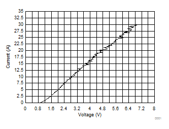
| RDYN | Dynamic on-resistance D1, D2 IEC clamps(4) | Dx to GND | 0.2 | Ω | ||
| GND to Dx | ||||||
(1) Pulsed testing techniques maintain junction temperature approximately equal to ambient temperature
(2) See Current Limit for explanation of this parameter.
(3) These Parameters are provided for reference only, and do not constitute a part of TI’s published device specifications for purposes of TI’s product warranty.
(4) RDYN was extracted using the least squares first of the TLP characteristics between I = 20 A and I = 30 A.
7.6 Electrical Characteristics: –40°C ≤ TJ ≤ 125°C
Unless otherwise noted: 4.5 V ≤ VIN ≤ 5.5 V, VEN = VIN, IOUT = 0 A, typical values are at 5 V and 25°C. See the Device Comparison Table for the rated current of each part number.| PARAMETER | TEST CONDITIONS(1) | MIN | TYP | MAX | UNIT | |
|---|---|---|---|---|---|---|
| POWER SWITCH | ||||||
| RDS(on) | Input – output resistance | TPD3S014 | 97 | 154 | mΩ | |
| TPD3S044 | 74 | 121 | ||||
| ENABLE INPUT (EN) | ||||||
| Threshold | Input rising | 1 | 1.45 | 2 | V | |
| Hysteresis | 0.13 | V | ||||
| Leakage current | VEN = 0 V | –1 | 0 | 1 | µA | |
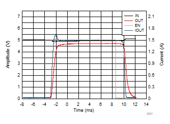
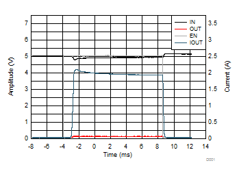
| tON | Turn on time | VIN = 5 V, CL = 1 µF, RL = 100 Ω, EN ↑ See Figure 26 |
1 | 1.6 | 2.2 | ms |
| tOFF | Turn off time | VIN = 5 V, CL = 1 µF, RL = 100 Ω, EN ↓ See Figure 26 |
1.7 | 2.1 | 2.7 | ms |
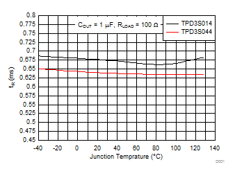
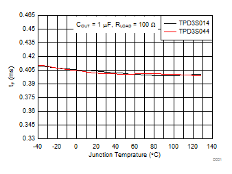
| tR | Rise time, output | CL = 1 µF, RL = 100 Ω, VIN = 5 V, See Figure 25 | 0.4 | 0.64 | 0.9 | ms |
| tF | Fall time, output | CL = 1 µF, RL = 100 Ω, VIN = 5 V, See Figure 25 | 0.25 | 0.4 | 0.8 | ms |
| CURRENT LIMIT | ||||||
| IOS(2) | Current limit, see Figure 27 | TPD3S014 | 0.65 | 0.85 | 1.05 | A |
| TPD3S044 | 1.60 | 2.15 | 2.70 | |||
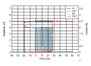
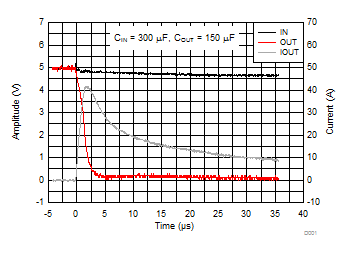
| tIOS | Short-circuit response time(3) | VIN = 5 V (see Figure 27) One Half full load → RSHORT = 50 mΩ Measure from application to when current falls below 120% of final value |
2 | µs | ||
| SUPPLY CURRENT | ||||||
| ISD | Supply current, switch disabled | IOUT = 0 A | 0.02 | 10 | µA | |
| ISE | Supply current, switch enabled | IOUT = 0 A | 66 | 94 | µA | |
| IREV | Reverse leakage current | VOUT = 5.5 V, VIN = 0 V, Measure IVOUT | 0.2 | 20 | µA | |
| UNDERVOLTAGE LOCKOUT | ||||||
| VUVLO | Rising threshold | VIN↑ | 3.5 | 3.77 | 4 | V |
| Hysteresis | VIN↓ | 0.14 | V | |||
| OUTPUT DISCHARGE | ||||||
| RPD | Output pull-down resistance | VIN = 4 V, VOUT = 5 V, Disabled | 350 | 545 | 1200 | Ω |
| VIN = 5 V, VOUT = 5 V, Disabled | 300 | 456 | 800 | |||
| THERMAL SHUTDOWN | ||||||
| TSHDN | Rising threshold (TJ) | In current limit | 135 | °C | ||
| Not in current limit | 155 | |||||
| Hysteresis(3) | 20 | °C | ||||
| ESD PROTECTION | ||||||
| II | Input leakage current (D1, D2) | VI = 3.3 V | 0.02 | 1 | µA | |
| VD | Diode forward voltage (D1, D2); Lower clamp diode | IO = 8 mA | 0.95 | V | ||
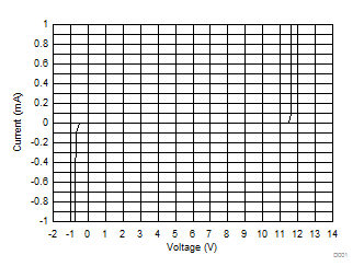
| VBR | Breakdown voltage (D1, D2) | IBR = 1 mA | 6 | V | ||
(1) Pulsed testing techniques maintain junction temperature approximately equal to ambient temperature
(2) See Current Limit section for explanation of this parameter.
(3) These parameters are provided for reference only, and do not constitute part of TI’s published device specifications for purposes of TI’s product warranty.
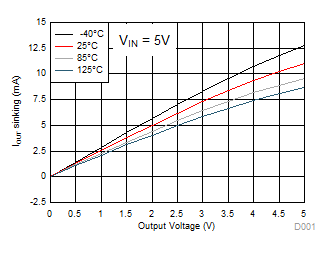
7.7 Typical Characteristics
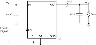
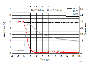
1. During the short applied tests, 300µF is used because of the use of an external supply.
Figure 1. Test Circuit for System Operation in Typical Characteristics
