SLUSDH1B may   2020  – april 2023 TPD3S713-Q1 , TPD3S713A-Q1

PRODUCTION DATA  

  1. Features
  2. Applications
  3. Description
  4. Revision History
  5. Pin Configuration and Functions
  6. Specifications
    1. 6.1 Absolute Maximum Ratings
    2. 6.2 ESD Ratings
    3. 6.3 Recommended Operating Conditions
    4. 6.4 Thermal Information
    5. 6.5 Electrical Characteristics
    6. 6.6 Switching Characteristics
    7. 6.7 Typical Characteristics
  7. Parameter Measurement Information
  8. Detailed Description
    1. 8.1 Overview
    2. 8.2 Functional Block Diagram
    3. 8.3 Feature Description
      1. 8.3.1 FAULT Response
      2. 8.3.2 Cable Compensation
        1. 8.3.2.1 Design Procedure
      3. 8.3.3 DP and DM Protection
      4. 8.3.4 VBUS OVP Protection
      5. 8.3.5 Output and DP or DM Discharge
      6. 8.3.6 Overcurrent Protection
      7. 8.3.7 Undervoltage Lockout
      8. 8.3.8 Thermal Sensing
      9. 8.3.9 Current-Limit Setting
    4. 8.4 Device Functional Modes
      1. 8.4.1 Device Truth Table (TT)
      2. 8.4.2 Client Mode
      3. 8.4.3 High-Bandwidth Data-Line Switch
  9. Application and Implementation
    1. 9.1 Application Information
    2. 9.2 Typical Application
      1. 9.2.1 Design Requirements
      2. 9.2.2 Detailed Design Procedure
        1. 9.2.2.1 Input Capacitance
        2. 9.2.2.2 Output Capacitance
        3. 9.2.2.3 BIAS Capacitance
        4. 9.2.2.4 Output and BIAS TVS
      3. 9.2.3 Application Curves
    3. 9.3 Power Supply Recommendations
    4. 9.4 Layout
      1. 9.4.1 Layout Guidelines
      2. 9.4.2 Layout Example
  10. 10Device and Documentation Support
    1. 10.1 Documentation Support
      1. 10.1.1 Related Documentation
    2. 10.2 Receiving Notification of Documentation Updates
    3. 10.3 Support Resources
    4. 10.4 Trademarks
    5. 10.5 Electrostatic Discharge Caution
    6. 10.6 Glossary
  11. 11Mechanical, Packaging, and Orderable Information

Package Options

Refer to the PDF data sheet for device specific package drawings

Mechanical Data (Package|Pins)
  • RVC|20
Thermal pad, mechanical data (Package|Pins)
Orderable Information

Client Mode

The TPD3S713x-Q1 device integrates client mode as shown in Figure 8-4. The internal power switch is OFF to block current flow from BUS to IN, and the signal switches are ON. This mode can be used for software upgrades from the USB port.
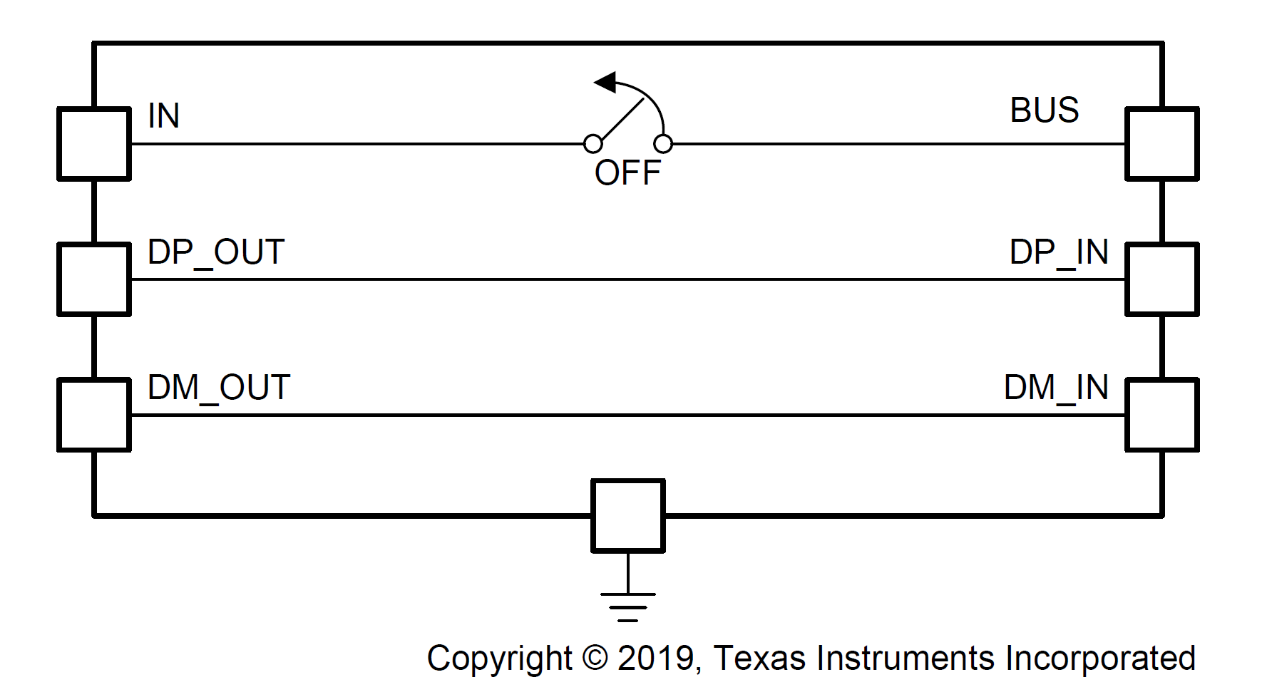
GUID-F8FAAB9D-F7FF-4892-A4E5-EF43A11EE6EB-low.pngFigure 8-4 Client-Mode Equivalent Circuit

In client mode, because the power switch is OFF, BUS must be 5 V so that the device can work normally (usually powered by an external downstream USB port). If the BUS voltage is low, the communication may not work properly.