SLVSDH9D March 2016 – August 2020 TPD3S716-Q1
PRODUCTION DATA
- 1 Features
- 2 Applications
- 3 Description
- 4 Revision History
- 5 Pin Configuration and Functions
- 6 Specifications
- 7 Parameter Measurement Information
-
8 Detailed Description
- 8.1 Overview
- 8.2 Functional Block Diagram
- 8.3
Feature Description
- 8.3.1 AEC-Q100 Qualified
- 8.3.2 Short-to-Battery and Short-to-Ground Protection on VBUS_CON
- 8.3.3 Short-to-Battery and Short-to-VBUS Protection on VD+, VD–
- 8.3.4 ESD Protection on VBUS_CON, VD+, VD–
- 8.3.5 Low RON nFET VBUS Switch
- 8.3.6 High Speed Data Switches
- 8.3.7 Adjustable Hiccup Current Limit up to 2.4-A
- 8.3.8 Fast Over-Voltage Response Time
- 8.3.9 Independent VBUS and Data Enable Pins for Configuring both Host and Client/OTG Mode
- 8.3.10 Fault Output Signal
- 8.3.11 Thermal Shutdown Feature
- 8.3.12 16-Pin SSOP Package
- 8.3.13 Reverse Current Detection
- 8.4 Device Functional Modes
- 9 Application and Implementation
- 10Power Supply Recommendations
- 11Layout
- 12Device and Documentation Support
- 13Mechanical, Packaging, and Orderable Information
Package Options
Mechanical Data (Package|Pins)
- DBQ|16
Thermal pad, mechanical data (Package|Pins)
Orderable Information
3 Description
The TPD3S716-Q1 is a single-chip solution for short-to-battery, short-circuit, and ESD protection with an adjustable current-limit for the USB connector’s VBUS and data lines in automotive applications. The integrated data switches provide best-in-class bandwidth for minimal signal degradation while simultaneously providing 18 V short-to-battery protection. The high bandwidth of 1 GHz allows for USB2.0 high-speed data rates for applications like Car Play. Extra margin in bandwidth above 720-MHz also helps to maintain a clean USB 2.0 eye diagram with the long captive cables that are common in the automotive USB environment. The short-to-battery protection isolates the internal system circuits from any over-voltage conditions at the VBUS_CON, VD+, and VD– pins. On these pins, the TPD3S716-Q1 can handle over-voltage protection up to 18 V for hot plug and DC events. The over-voltage protection circuit provides the most reliable short-to-battery isolation in the industry, shutting off the data switches in 200 ns and protecting the upstream circuitry from harmful voltage and current spikes.
The VBUS_CON pin also provides an adjustable current limited load switch and handles short-to-ground protection. The device supports VBUS currents up to 2.4 A, allowing support for charging USB BC1.2, USB Type-C 5V/1.5A, and proprietary charging schemes up to 2.4 A. The separate enable pins for data and VBUS allow for both host and client-OTG mode. TPD3S716-Q1 also integrates system level IEC 61000-4-2 and ISO 10605 ESD protection on its VBUS_CON, VD+, and VD– pins removing the need to provide external high voltage, low capacitance diodes.
| PART NUMBER | PACKAGE | BODY SIZE (NOM) |
|---|---|---|
| TPD3S716-Q1 | SSOP (16) | 4.90 mm × 3.90 mm |
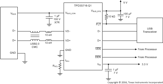
 Typical Application Schematic