SLVSC54B July 2013 – April 2014 TPD4E110
PRODUCTION DATA.
- 1 Features
- 2 Applications
- 3 Description
- 4 Simplified Schematic
- 5 Revision History
- 6 Terminal Configuration and Functions
- 7 Specifications
- 8 Detailed Description
- 9 Applications and Implementation
- 10Layout
- 11Device and Documentation Support
- 12Mechanical, Packaging, and Orderable Information
Package Options
Mechanical Data (Package|Pins)
- DPW|4
Thermal pad, mechanical data (Package|Pins)
- DPW|4
Orderable Information
10 Layout
10.1 Layout Guidelines
- The optimum placement is as close to the connector as possible.
- EMI during an ESD event can couple from the trace being struck to other nearby unprotected traces, resulting in early system failures.
- The PCB designer needs to minimize the possibility of EMI coupling by keeping any unprotected traces away from the protected traces which are between the TVS and the connector.
- Route the protected traces as straight as possible.
- Eliminate any sharp corners on the protected traces between the TVS and the connector by using rounded corners with the largest radii possible.
- Electric fields tend to build up on corners, increasing EMI coupling.
10.2 Layout Example
10.2.1 Single Layer Routing
PCB manufacturing technologies allowing 2.8 mil (0.071 mm) clearances can route two Super-Speed data line pairs through TPD4E110 on a single layer.
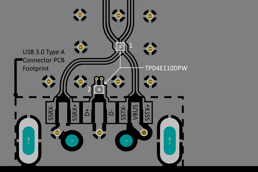 Figure 15. Example Layout for USB 3.0 Type A connector using two TPD4E110s
In Figure 15, Figure 16 and Figure 17 an example layout shows the use of two TPD4E110s to protect the USB 3.0 port. TPD4E110 Number 1 is protecting the two Super-Speed data pairs used for Super Speed data transfer, and TPD4E110 Number 2 protects the USB 2.0 D+/D– Hi-Speed data lines. Number 2 uses two channels to protect each line in the pair, thus affording a more robust protection and simpler layout.
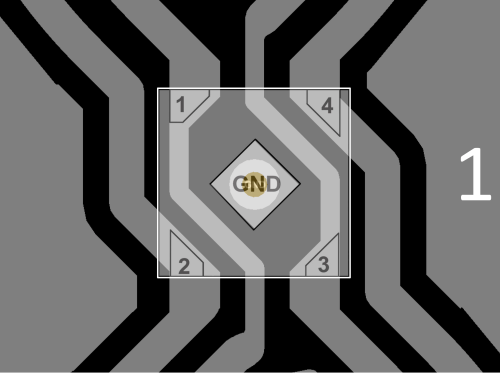 Figure 16. Close-up of Routing for TPD4E110 for Super-Speed Data Lines
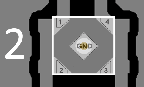 Figure 17. Close-up of Routing for TPD4E110 for USB 2.0 D+/D– Hi-Speed Data Lines
10.2.2 Double Layer Routing
PCB manufacturing technologies allowing 4.0 mil (0.1 mm) clearances can route two Super-Speed data line pairs through TPD4E110 using two layers.
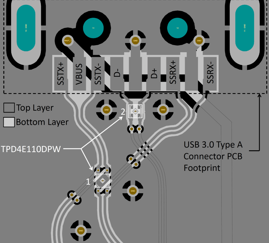 Figure 18. Example Layout for USB 3.0 Type A Connector Using Two TPD4E110s
In Figure 18 an example layout shows the use of two TPD4E110s to protect the USB 3.0 port. TPD4E110 Number 1 is protecting the two Super-Speed data pairs used for high speed data transfer, and TPD4E110 Number 2 protects the USB 2.0 D+/D– Hi-Speed lines. Number 2 uses two channels to protect each line in the pair, thus affording a more robust protection and simpler layout.