SLLS800B June 2010 – May 2021 TPD4F202 , TPD6F202
PRODUCTION DATA
- 1 Features
- 2 Applications
- 3 Description
- 4 Revision History
- 5 Pin Configuration and Functions
- 6 Specifications
- 7 Detailed Description
- 8 Application and Implementation
- 9 Power Supply Recommendations
- 10Layout
- 11Device and Documentation Support
- 12Mechanical, Packaging, and Orderable Information
Package Options
Mechanical Data (Package|Pins)
- YFU|15
Thermal pad, mechanical data (Package|Pins)
Orderable Information
3 Description
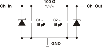
The TPDxF202 devices are four or six-channel EMI filters, designed particularly to suppress EMI noise in the cell phone and other portable applications. These filters also provide a Transient Voltage Suppressor (TVS) diode circuit for Electrostatic Discharge (ESD) protection which prevents damage to the application when subjected to ESD stress far exceeding IEC 61000-4-2 (Level 4). The pi-style C-R-C filter provides symmetric filter performance in the data lines to and from either side of the filter.
Due to the tiny parasitics of the DSBGA package, the TPDxF202 filters provide excellent signal attenuation (–40 dB at 1 GHz) at the typical cell-phone carrier frequency ranges.
The ultra thin (0.3-mm package height, when mounted on board) space-saving YFU package enables the TPDxF202 devices to mount on the printed-circuit-boards where height is a key constraint.
The TPDxF202 devices are specified for –40°C to 85°C operation.
A typical application for TPDxF202 devices are in portable equipment with DVI, VGA, SVGA, SIM Card, and other data interfaces.
| PART NUMBER | PACKAGE | BODY SIZE (NOM) |
|---|---|---|
| TPD4F202 | DSBGA (10) | 1.06 mm × 1.57 mm |
| TPD6F202 | DSBGA (15) | 1.06 mm × 2.36 mm |
 Functional Block Diagram