SLIS140A October 2011 – December 2014 TPIC74101-Q1
PRODUCTION DATA.
- 1 Features
- 2 Applications
- 3 Description
- 4 Revision History
- 5 Pin Configuration and Functions
- 6 Specifications
-
7 Detailed Description
- 7.1 Overview
- 7.2 Functional Block Diagram
- 7.3
Feature Description
- 7.3.1 Switch-Mode Input/Output Pins (L1, L2)
- 7.3.2 Supply Pin (Vdriver)
- 7.3.3 Internal Supply Decoupling Pin (Vlogic)
- 7.3.4 Input Voltage Monitoring Pin (AIN)
- 7.3.5 Input Undervoltage Alarm Pin (AOUT)
- 7.3.6 Reset Delay Timer Pin (REST)
- 7.3.7 Reset Pin (RESET)
- 7.3.8 Main Regulator Output Pin (VOUT)
- 7.3.9 Low-Power-Mode Pin (CLP)
- 7.3.10 Switch-Output Pin (5Vg)
- 7.3.11 5Vg-Enable Pin (5Vg_ENABLE)
- 7.3.12 Slew-Rate Control Pins (SCR0, SCR1)
- 7.3.13 Modulator Frequency Setting (Pin Rmod)
- 7.3.14 Ground Pin (PGND)
- 7.3.15 Enable Pin (ENABLE)
- 7.3.16 Bootstrap Pins (Cboot1 and Cboot2)
- 7.4 Device Functional Modes
- 8 Application and Implementation
- 9 Power Supply Recommendations
- 10Layout
- 11Device and Documentation Support
- 12Mechanical, Packaging, and Orderable Information
Package Options
Mechanical Data (Package|Pins)
- PWP|20
Thermal pad, mechanical data (Package|Pins)
- PWP|20
Orderable Information
6 Specifications
6.1 Absolute Maximum Ratings
over recommended operating free-air temperature range (unless otherwise noted)(1)| MIN | MAX | UNIT | ||
|---|---|---|---|---|
| Unregulated input voltage, V(driver)(2) | –0.5 | 40 | V | |
| Unregulated inputs, V(AIN), V(ENABLE)(2) | –0.5 | 40 | V | |
| Bootstrap voltages | V(Cboot1) | 52 | V | |
| V(Cboot2) | 14 | V | ||
| Switch mode voltages | V(L1) | –1 | 40 | V |
| V(L2) | –1 | 7 | V | |
| Logic input voltages, V(Rmod),V(SCR0),V(SCR1),V(CLP), and V(5Vg_ENABLE) (2) | –0.5 | 7 | V | |
| Low output voltages, V(RESET),V(AOUT),V(logic), and V(REST)(2) | –0.5 | 7 | V | |
| Continuous power dissipation, PD | See Dissipation Rating | |||
| Operating virtual junction temperature range, TJ | –40 | 150 | °C | |
| Operating ambient temperature range, TA | –40 | 125 | °C | |
| Lead temperature (soldering, 10 s), T(LEAD) | 260 | °C | ||
| Storage temperature, Tstg | –65 | 125 | °C | |
(1) Stresses beyond those listed under Absolute Maximum Ratings may cause permanent damage to the device. These are stress ratings only, and functional operation of the device at these or any other conditions beyond those indicated under Recommended Operating Conditions is not implied. Exposure to absolute-maximum-rated conditions for extended periods may affect device reliability.
(2) All voltage values are with respect to ground.
6.2 ESD Ratings
| VALUE | UNIT | |||||
|---|---|---|---|---|---|---|
| V(ESD) | Electrostatic discharge | Human body model (HBM), per JEDEC | Pin 7 (L2), pin 8 (VOUT), Pin 9 (5Vg) | ±800 | V | |
| Pins 1–6 and 10–20 | ±2000 | |||||
| Charged device model (CDM), per JEDEC | Corner pins (SCR1, AIN, SCR0, and CLP) | ±750 | ||||
| Other pins | ±750 | |||||
6.3 Recommended Operating Conditions
| MIN | NOM | MAX | UNIT | ||
|---|---|---|---|---|---|
| Unregulated input voltage, V(driver) | 6 | 24 | V | ||
| Unregulated input voltages, V(AIN) and V(ENABLE) | 0 | 24 | V | ||
| Switch-mode pins | V(L1) | –1 | 17 | V | |
| V(L2) | 5 | 5.5 | |||
| Bootstrap voltages | V(Cboot1) | V(driver) + 10 | V | ||
| V(Cboot2) | 8 | ||||
| Logic levels (I/O), V(Rmod), V(logic),V(SCR0),V(SCR1),V(5Vg_ENABLE),V(RESET), V(AOUT), V(CLP), and V(REST) | 0 | 5.25 | V | ||
| Operating ambient temperature range, TA | –40 | 125 | °C | ||
| Logic levels (I/O), V(SCR0), V(SCR1), V(CLP) directly connected to V(logic) | V(logic) | V(logic) | V | ||
6.4 Thermal Information
| THERMAL METRIC(1) | TPIC74101-Q1 | UNIT | |
|---|---|---|---|
| PWP | |||
| 20 PINS | |||
| RθJA(2) | Junction-to-ambient thermal resistance | 32 | °C/W |
| RθJA(3) | Junction-to-ambient thermal resistance | 37.9 | |
| RθJC(top) | Junction-to-case (top) thermal resistance | 22.7 | |
| RθJB | Junction-to-board thermal resistance | 20.2 | |
| ψJT | Junction-to-top characterization parameter | 0.7 | |
| ψJB | Junction-to-board characterization parameter | 19.9 | |
| RθJC(bot) | Junction-to-case (bottom) thermal resistance | 1.8 | |
(1) For more information about traditional and new thermal metrics, see the IC Package Thermal Metrics application report, SPRA953.
(2) The thermal data is based on using 2-oz copper trace with at least four square inches of copper footprint for heat dissipation. The copper pad is soldered to the thermal land pattern. Correct attachment procedure must be incorporated.
(3) The thermal data is based on using 1-oz copper trace with at least four square inches of copper footprint for heat dissipation. The copper pad is soldered to the thermal land pattern. Correct attachment procedure must be incorporated.
6.5 Dissipation Rating
| RθJA | TA ≤ 25°C POWER RATING |
DERATING FACTOR ABOVE TA = 25°C |
TA = 85°C POWER RATING |
TA = 125°C POWER RATING |
|---|---|---|---|---|
| 32°C/W | 3.9 W | 31.25 mW/°C | 2.03 W | 0.781 W |
| 40°C/W | 3.125 W | 25 mW/°C | 1.625 W | 0.625 W |
6.6 Electrical Characteristics
V(driver) = 6 V to 17 V, TA = -40°C to 125°C, unless otherwise noted| PARAMETERS | TEST CONDITIONS | MIN | TYP | MAX | UNIT | |
|---|---|---|---|---|---|---|
| V(driver) | Unregulated input voltage | 1.5 | 40 | V | ||
| V(driver) | Start-up condition voltage | IO = 600 mA | 5 | V | ||
| SOM | Soft-start ramp | CO = 36 μF (min) to 220 μF (max) | 4 | 20 | V/ms | |
| CO = 220 μF (min) to 470 μF (max)(1) | 2 | 20 | ||||
| I(standby) | Standby current | ENABLE = low | 10 | 20 | μA | |
| Iq | Quiescent current | CLP = 0 V, V(driver) = 11 V, IO = 0 mA | 110 | 160 | μA | |
| VO | Output voltage | DC | 5 | V | ||
| VO | Output-voltage tolerance | Buck mode | 2% | |||
| Low-Power or Boost or Boost/buck crossover mode | 3% | |||||
| IO | Output current | V(driver)≥ 7 V | 1 | A | ||
| IO(Boost) | Output current, boost mode | V(driver) = 2 V, see Note (2) | 200 | mA | ||
| V(driver)= 1.5 V, see Note (2) | 120 | |||||
| IPPn | Internal peak current limit (normal mode) | (1) | 1.75 | 2.5 | A | |
| IPPl | Internal peak current limit (low-power mode) | (1) | 0.75 | 1.25 | A | |
| IP | Peak current | V(driver) = 16 V, IO = 1 A, and L = 33 μH | 1.5 | A | ||
| V(driver) | Boost/buck crossover voltage window | See Note (3) | 5 | 5.9 | V | |
| Tot | Thermal shutdown(4) | 160 | 180 | 200 | °C | |
| 5Vg OUTPUT AND ENABLE | ||||||
| rDS(on) | On-state resistance | 140 | 225 | mΩ | ||
| IO | Output current | 400 | mA | |||
| VI | 5Vg_ENABLE input-voltage range | –0.5 | VO | V | ||
| VIH | 5Vg_ENABLE threshold high voltage | V(5Vg) = 5 V | 2.5 | 3 | 3.5 | V |
| VIL | 5Vg_ENABLE threshold low voltage | V(5Vg) = 0 V | 1.5 | 2 | 2.5 | V |
| V(hys) | Hysteresis voltage | 0.5 | 1 | V | ||
| r(pd) | Internal pulldown resistor | 300 | 500 | 850 | kΩ | |
| ENABLE | ||||||
| VI | ENABLE input-voltage range | –0.5 | 40 | V | ||
| VIH | ENABLE threshold high voltage | 8 V ≤ V(driver) ≤ 17 V | 2.5 | 3 | 3.5 | V |
| 6 V ≤ V(driver) < 8 V | 1.9 | 2.5 | 3.5 | |||
| VIL | ENABLE threshold low voltage | VO = 5 V | 1.5 | 1.85 | 2.5 | V |
| V(hys) | Hysteresis voltage | 8 V ≤ V(driver) ≤ 17 V | 0.5 | 1 | V | |
| 6 V ≤ V(driver) < 8 V | 0.1 | |||||
| RESET | ||||||
| V(th) | RESET threshold voltage | 4.51 | 4.65 | 4.79 | V | |
| V(RESET) | RESET tolerance | 3% | ||||
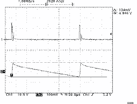
| t(RESET) | RESET time | C(REST) = 10 nF | 8 | 10 | 12 | ms |
| C(REST)= 100 nF, see Note (1) | 80 | 100 | 120 | |||
| VOL | RESET output low voltage | Isink = 5 mA | 450 | mV | ||
| Isink = 1 mA | 84 | |||||
| t(deglitch) | RESET deglitch time | See Note(1) | 8 | 10 | 12.5 | μs |
| ALARM | ||||||
| VI | Alarm input-voltage range | –0.5 | 40 | V | ||
| VIL | Alarm threshold low voltage | 2.2 | 2.3 | 2.35 | V | |
| VIH | Alarm threshold high voltage | 2.43 | 2.5 | 2.58 | V | |
| V(hys) | Hysteresis voltage | 240 | mV | |||
| VOL | Alarm output low voltage | Isink = 5 mA | 450 | mV | ||
| Isink = 1 mA | 84 | |||||
| LOW-POWER MODE (PULSE MODE) PFM | ||||||
| IO(LPM) | Load current in low-power mode | V(driver) < 7 V | 50 | mA | ||
| II(avg) | Average input current | V(driver) = 11 V, IO = 5 mA, CLP = low | 3.55 | mA | ||
| VO | Output-voltage tolerance | VO = 5 V | 2.4% | 3% | ||
| DIGITAL LOW-POWER MODE (CLP) | ||||||
| VIH | High-level CLP input threshold voltage | Normal mode | 2.6 | V | ||
| VIL | Low-level CLP input threshold voltage | Low-power mode | 1.15 | V | ||
| SWITCHING PARAMETERS | ||||||
| f(sw) | Switching frequency | V(Rmod) = 0 V, modulator OFF | 380 | kHz | ||
| f(sw)ac | Operating-frequency accuracy | f(sw) = 380 kHz | 20% | |||
| f(sw)min | Modulation minimum frequency | 230 | 285 | 385 | kHz | |
| f(sw)max | Modulation maximum frequency | 390 | 480 | 590 | kHz | |
| f(mod)span | Modulation span | 220 | kHz | |||
| f(mod) | Modulation frequency | Rmod = 12 kΩ ±1% | 28 | kHz | ||
| f(mod)ac | Modulation-frequency accuracy | 12% | ||||
(1) Ensured by characterization
(2) Tested with inductor having following characteristics: L = 33 μH, Rmax = 0.1 Ω, IR = 1.8 A. Output current must be verified in application when inductor Rmax (ESR) is increased.
(3) Ensured by characterization. For further details, see the Buck/Boost Transitioning section.
(4) Ensured by characterization; hysteresis 15°C (typical)
6.7 Typical Characteristics
(Reference L1 Pin, see Figure 10 through Figure 12)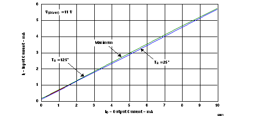
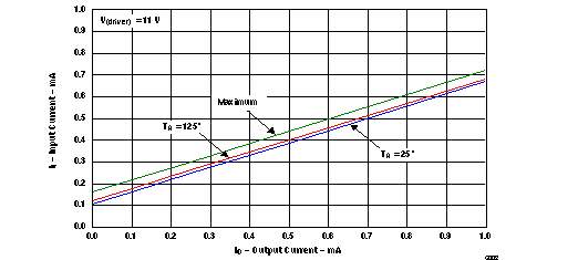
| Maximum characteristic specified by design. | ||
| IO = 0 mA–10 mA | ||
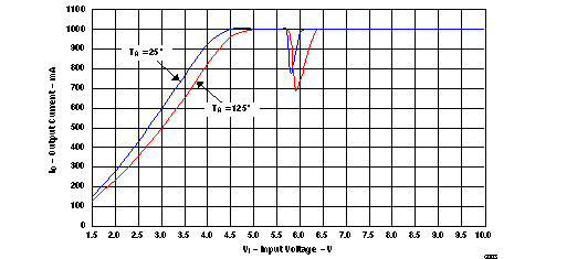
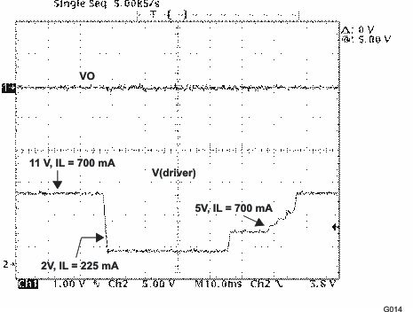
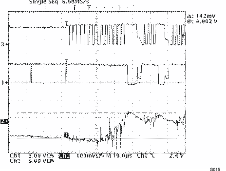
| (1) Typical representation of input voltage vs output load current at TA = 25°C and 125°C, after the correct power-up sequence is invoked. | ||
| (2) The dip in the output current at 5.8 V is caused by the buck/boost transition of the IC. | ||
| (3) The output current is clipped to 1 A by the measurement setup. |
Maximum Output Load Current (IO)
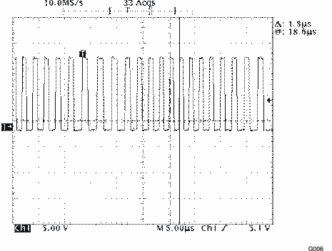
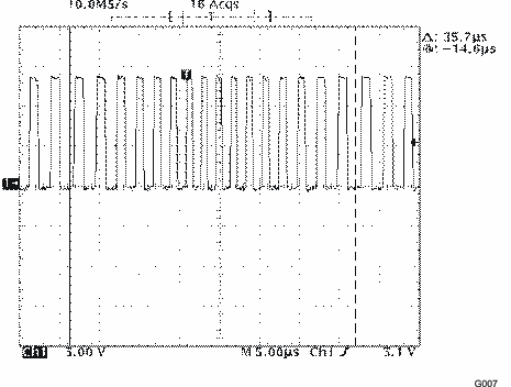
| SCR1 = 0, SCR0 = 1, Input-Current Slew Rate = 6.25 A/μs, | ||
| IL = 500 mA, V(driver) = 15 V |
| SCR0 = 1, SCR1 = 1, Input-Current Slew Rate = 18.8 A/μs, | ||
| IL = 500 mA, V(driver) = 15 V |
| IL = 200 mA |
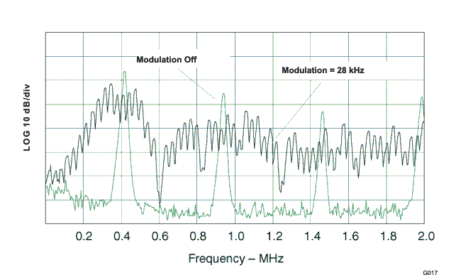
(446 kHz) with Modulation Function Disabled
| Rmod = 12 kΩ, IL = 200 mA |
with Modulation Enabled
| IL = 400 mA | ||
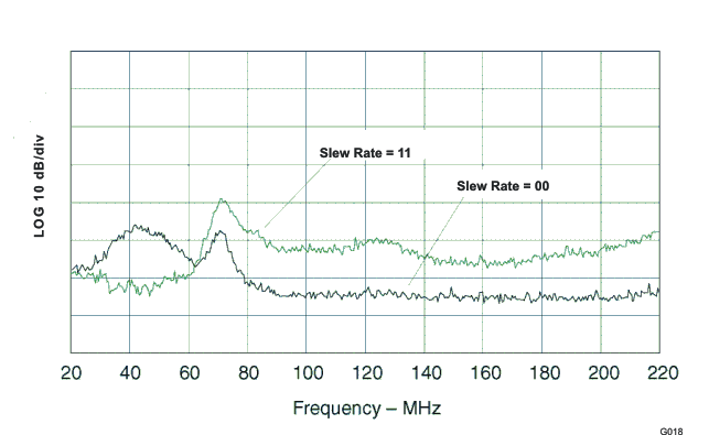
| These values represent conducted EMI results of a test board for display purposes only. Actual results may vary greatly depending on board layout and external components and must be verified in actual application. |
| Maximum characteristic specified by design. | ||
| IO = 0 mA–1 mA | ||
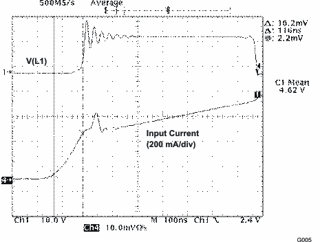
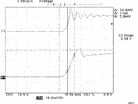
\
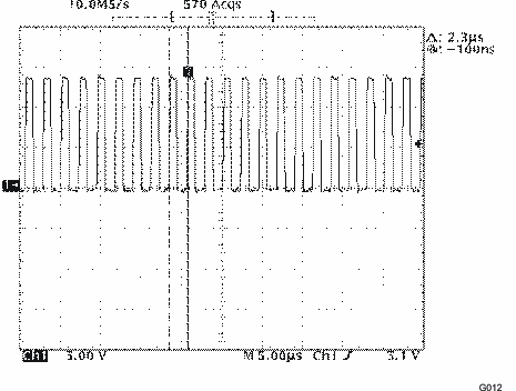
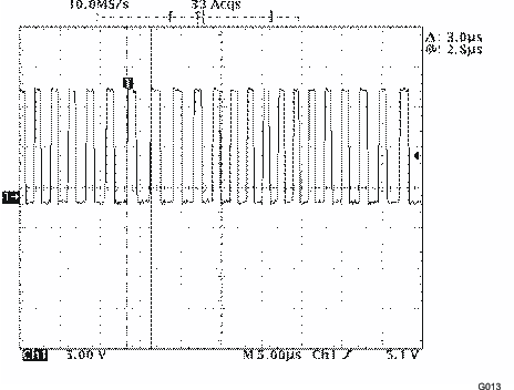
Figure 4. Input Current With Slope Control
| SCR0 = 0, SCR1 = 0, Input-Current Slew Rate = 2.8 A/μs, | ||
| IL = 500 mA, V(driver) = 15 V | ||
| SCR1 = 1, SCR0 = 0, Input-Current Slew Rate = 9.4 A/μs, | ||
| IL = 500 mA, V(driver) = 15 V |
| IL = 15 mA, CO = 47 μF | ||
| Rmod = 12 kΩ, IL = 200 mA |
With Modulation Enabled
| IL = 400 mA |
.
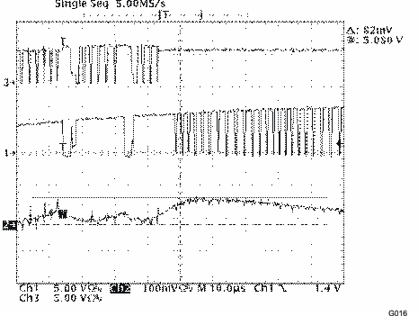
Figure 16. Conducted Emissions on Test Board Showing Effects of Switching-Frequency Modulation
| These values represent conducted EMI results of a test board for display purposes only. Actual results may vary greatly depending on board layout and external components and must be verified in actual application |