SLIS149 June 2014 TPL0102-EP
PRODUCTION DATA.
- 1 Features
- 2 Applications
- 3 Description
- 4 Functional Block Diagram
- 5 Revision History
- 6 Pin Configuration and Functions
- 7 Specifications
-
8 Detailed Description
- 8.1 Overview
- 8.2 Functional Block Diagram
- 8.3 Feature Description
- 8.4 Device Functional Modes
- 8.5
Register Maps
- 8.5.1 Slave Address
- 8.5.2 TPL0102-EP Register Maps
- 8.5.3 IVRA (Initial Value Register for Potentiometer A)
- 8.5.4 WRA (Wiper Resistance Register for Potentiometer A)
- 8.5.5 IVRB (Initial Value Register for Potentiometer B)
- 8.5.6 WRB (Wiper Resistance Register for Potentiometer B)
- 8.5.7 ACR (Access Control Register)
- 9 Application and Implementation
- 10Layout
- 11Device and Documentation Support
- 12Mechanical, Packaging, and Orderable Information
Package Options
Mechanical Data (Package|Pins)
- PW|14
Thermal pad, mechanical data (Package|Pins)
Orderable Information
7 Specifications
7.1 Absolute Maximum Ratings(1)(2)(3)
| MIN | MAX | UNIT | |||
|---|---|---|---|---|---|
| VDD to GND | Supply voltage | –0.3 | 7 | V | |
| VSS to GND | –7 | 0.3 | V | ||
| VDD to VSS | 7 | V | |||
| VH, VL, VW | Voltage at resistor pins | VSS – 0.3 | VDD + 0.3 | V | |
| VI | Digital input voltage | –0.3 | VDD + 0.3 | V | |
| IH, IL, IW
|
Pulse current | ±20 | mA | ||
| Continuous current | ±2 | mA | |||
(1) Stresses above these ratings may cause permanent damage. Exposure to absolute maximum conditions for extended periods may degrade device reliability. These are stress ratings only, and functional operation of the device at these or any other conditions beyond those specified is not implied.
(2) The algebraic convention, whereby the most negative value is a minimum and the most positive value is a maximum.
(3) All voltages are with respect to ground, unless otherwise specified.
7.2 Handling Ratings
| MIN | MAX | UNIT | ||
|---|---|---|---|---|
| Tstg | Storage temperature range | –65 | 150 | °C |
7.3 Recommended Operating Conditions
over operating free-air temperature range (unless otherwise noted)| MIN | MAX | UNIT | ||
|---|---|---|---|---|
| VDD, VSS | Single supply operation (VSS = 0 V) | 2.7 | 5.5 | V |
| Dual supply operation | ±2.25 | ±2.75 | ||
| VH, VL | Pin voltage | VSS | VDD | V |
| VIH | Voltage input high (SCL, SDA, A0, A1, A2) | 0.7 × VDD | 5.5 | V |
| VIL | Voltage input low (SCL, SDA, A0, A1, A2) | 0 | 0.3 × VDD | V |
| IW | Wiper current | ±2 | mA | |
| TJ | Junction temperature | –40 | 125 | °C |
7.4 Thermal Information
| THERMAL METRIC(1) | TPL0102-EP | UNIT | |
|---|---|---|---|
| PW | |||
| 14 PINS | |||
| RθJA | Junction-to-ambient thermal resistance(2) | 112.9 | °C/W |
| RθJC(top) | Junction-to-case (top) thermal resistance(3) | 39.9 | |
| RθJB | Junction-to-board thermal resistance(4) | 55.9 | |
| ψJT | Junction-to-top characterization parameter(5) | 3.5 | |
| ψJB | Junction-to-board characterization parameter(6) | 55.2 | |
| RθJC(bot) | Junction-to-case (bottom) thermal resistance(7) | N/A | |
(1) For more information about traditional and new thermal metrics, see the IC Package Thermal Metrics application report, SPRA953.
(2) The junction-to-ambient thermal resistance under natural convection is obtained in a simulation on a JEDEC-standard, high-K board, as specified in JESD51-7, in an environment described in JESD51-2a.
(3) The junction-to-case (top) thermal resistance is obtained by simulating a cold plate test on the package top. No specific JEDEC-standard test exists, but a close description can be found in the ANSI SEMI standard G30-88.
(4) The junction-to-board thermal resistance is obtained by simulating in an environment with a ring cold plate fixture to control the PCB temperature, as described in JESD51-8.
(5) The junction-to-top characterization parameter, ψJT, estimates the junction temperature of a device in a real system and is extracted from the simulation data for obtaining θJA, using a procedure described in JESD51-2a (sections 6 and 7).
(6) The junction-to-board characterization parameter, ψJB, estimates the junction temperature of a device in a real system and is extracted from the simulation data for obtaining θJA , using a procedure described in JESD51-2a (sections 6 and 7).
(7) The junction-to-case (bottom) thermal resistance is obtained by simulating a cold plate test on the exposed (power) pad. No specific JEDEC standard test exists, but a close description can be found in the ANSI SEMI standard G30-88.
7.5 Electrical Characteristics
VDD = 2.7 to 5.5 V, VSS = 0 V, VH= VDD, VL= GND, TJ = –40°C to 125°C (unless otherwise noted). Typical values are atVDD = 5 V, TJ = 25°C (unless otherwise noted).
| PARAMETER | TEST CONDITIONS | MIN | TYP | MAX | UNIT | |||
|---|---|---|---|---|---|---|---|---|
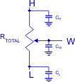
| RTOT | End-to-end resistance (Between H and L pins) |
TPL0102-100 | 80 | 100 | 120 | kΩ | ||
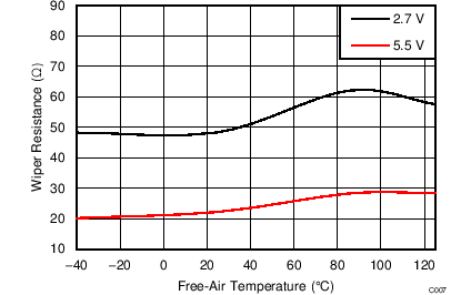
| RH, RL | Pin resistance | 60 | 200 | Ω | ||||
| RW | Wiper resistance | 25 | 120 | Ω | ||||
| CH, CL(14)(15) | Pin capacitance | 22 | pF | |||||
| CW(14)(15) | Wiper capacitance | 16 | pF | |||||
| ILKG | Pin leakage current | VH = VSS to VDD, VL = Floating or VL = VSS to VDD, VH = Floating |
0.1 | 1 | µA | |||
| TCR | Resistance temperature coefficient | Input Code = 0x80h | 92 | ppm/°C | ||||
| RTOT,MATCH | Channel-to-channel resistance match | 0.1 | % | |||||
| VOLTAGE DIVIDER MODE | ||||||||
| INL(1)(3) | Integral non-linearity | –0.5 | 0.5 | LSB | ||||
| DNL(1)(4) | Differential non-linearity | –0.25 | 0.25 | LSB | ||||
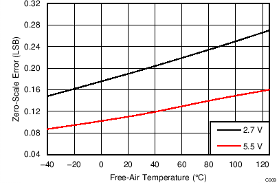
| ZSERROR(2)(5) | Zero-scale error | 0 | 0.1 | 2 | LSB | |||
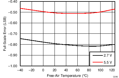
| FSERROR(2)(6) | Full-scale error | –2 | –0.1 | 0 | LSB | |||
| VMATCH(2)(7) | Channel-to-channel matching | Wiper at the same tap position, same voltage at all H and same voltage at all L pins | –2 | 2 | LSB | |||
| TCV | Ratiometric temperature coefficient | Wiper set at mid-scale | 4 | ppm/°C | ||||
| BW | Bandwidth | TPL0102-100 | Wiper set at midscale CLOAD = 10 pF |
229 | kHz | |||
| TSW | Wiper setting time | TPL0102-100 | 3.6 | µS | ||||
| THD | Total harmonic distortion | VH = 1 VRMS at 1 kHz, VL = (VDD – VSS)/2, Measurement at W |
TPL0102-100 | 0.03 | % | |||
| XTALK | Crosstalk | ƒH = 1 kHz, VL = GND, Measurement at W |
–82 | dB | ||||
| RHEOSTAT MODE (Measurements between W and L with H not connected, or between W and H with L not connected) | ||||||||
| RINL(8)(10) | Integral non-linearity | –1 | 1 | LSB | ||||
| RDNL(8)(11) | Differential non-linearity | –0.5 | 0.5 | LSB | ||||
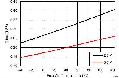
| ROFFSET(9)(12) | Offset | 0 | 0.2 | 2 | LSB | |||
| RMATCH(9)(13) | Channel-to-channel matching | –2 | 2 | LSB | ||||
| RBW | Bandwidth | Code = 0x00h, L Floating, Input applied to W, Measure at H, CLOAD = 10 pF |
TPL0102-100 | 54 | kHz | |||
(1) LSB = (VMEAS[code 255] – VMEAS[code 0]) / 255
(2) IDEAL_LSB = (VH – VL) / 256
(3) INL = ((VMEAS[code x] – VMEAS[code 0]) / LSB) – [code x]
(4) DNL = ((VMEAS[code x] – VMEAS[code x-1]) / LSB) – 1
(5) ZSERROR = VMEAS[code 0] / IDEAL_LSB
(6) FSERROR = [(VMEAS[code 255] – (VH – VL)) / IDEAL_LSB] + 1
(7) VMATCH = (VMEAS_A[code x] – VMEAS_B[code x]) / IDEAL_LSB
(8) RLSB = (RMEAS[code 255] – RMEAS[code 0]) / 255
(9) IDEAL_RLSB = RTOT / 256
(10) RINL =( (RMEAS[code x] – RMEAS[code 0]) / RLSB) – [code x]
(11) RDNL =( (RMEAS[code x] – RMEAS[code x-1]) / RLSB ) – 1
(12) ROFFSET = RMEAS[code 0] / IDEAL_RLSB
(13) RMATCH = (RMEAS_A[code x] – RMEAS_B[code x]) / IDEAL_RLSB
(14) Pin and wiper capacitance extracted from self admittance of three port network measurement
(15) Digital Potentiometer Macromodel
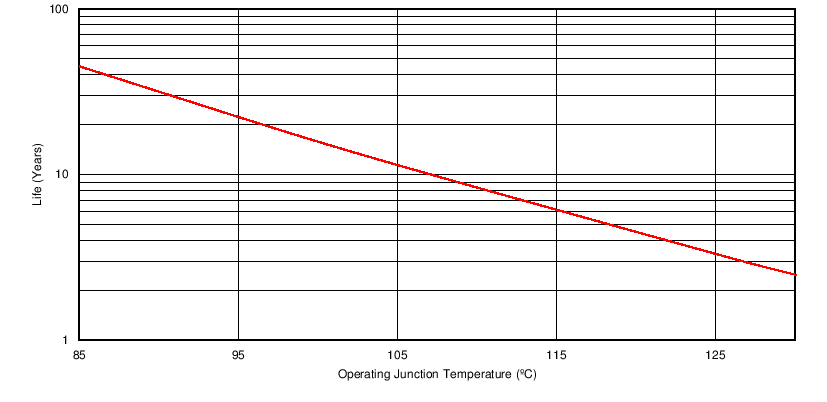
1. See data sheet for absolute maximum and minimum recommended operating conditions.
2. Silicon operating life design goal is 10 years at 105°C junction temperature (does not include package interconnect life).
3. Enhanced plastic product disclaimer applies.
Figure 1. TPL0102-EP Electromigration Fail Mode/Wirebond Life Derating Chart
7.6 Operating Characteristics
VDD = 2.7 to 5.5 V, VSS = 0 V, VH = VDD, VL = GND, TJ= –40°C to 125°C (unless otherwise noted). Typical values are atVDD = 5 V, TJ = 25°C (unless otherwise noted).
| PARAMETER | TEST CONDITIONS | MIN | TYP | MAX | UNIT | ||
|---|---|---|---|---|---|---|---|
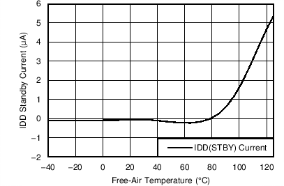
| IDD(STBY) | VDD standby current | VDD = 2.75 V, VSS = –2.75 V, I2C interface in standby mode |
–40°C | 0.2 | 1.5 | µA | |
| 25°C | 1 | ||||||
| 125°C | 16 | ||||||
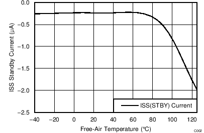
| ISS(STBY) | VSS standby current | VDD = 2.75 V, VSS = –2.75 V, I2C interface in standby mode |
–40°C | –1.5 | –0.2 | µA | |
| 25°C | –1 | ||||||
| 125°C | –16 | ||||||
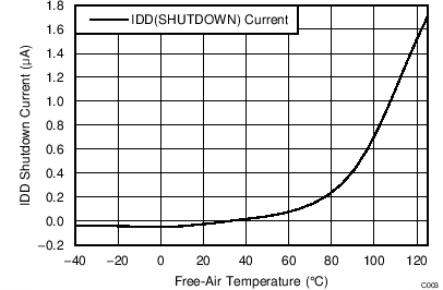
| IDD(SHUTDOWN) | VDD shutdown current | VDD = 2.75 V, VSS = –2.75 V, I2C interface in standby mode |
–40°C | 0.2 | 1.5 | µA | |
| 25°C | 1 | ||||||
| 125°C | 16 | ||||||
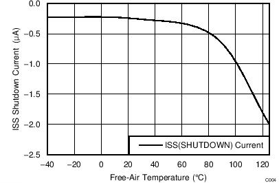
| ISS(SHUTDOWN) | VSS shutdown current | VDD = 2.75 V, VSS = –2.75 V, I2C interface in standby mode |
–40°C | –1.5 | –0.2 | µA | |
| 25°C | –1 | ||||||
| 125°C | –16 | ||||||
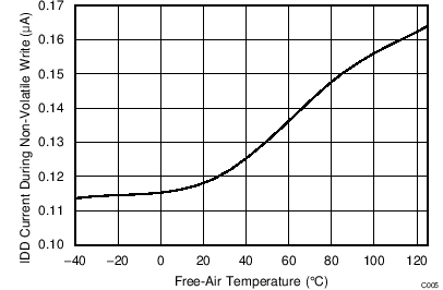
| IDD | VDD current during non-volatile write | VDD = 2.75 V, VSS = –2.75 V | 350 | µA | |||
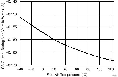
| ISS | VSS current during non-volatile write | VDD = 2.75 V, VSS = –2.75 V | -350 | µA | |||
| ILKG-DIG | Digital pins leakage current (A0, A1, A2, SDA, and SCL) | –1 | 1 | µA | |||
| VPOR | Power-on recall voltage | Minimum VDD at which memory recall occurs | 2 | V | |||
| EEPROM SPECIFICATION | |||||||
| EEPROM endurance | 1000 | Cycles | |||||
| EEPROM retention | 100000 | Hours | |||||
| tWC | Non-volatile write cycle time | 20 | ms | ||||
| WIPER TIMING CHARACTERISTICS | |||||||
| tWRT | Wiper response time | SCL falling edge of last bit of wiper data byte to wiper new position | 600 | ns | |||
| tSHUTDOWNREC | Wiper position recall time from shut-down mode | SCL falling edge of last bit of ACR data byte to wiper stored position and H connection | 800 | ns | |||
| tD | Power-up delay | VDD above VPOR, to wiper initial value register recall completed, and I2C interface in standby mode | 35 | 100 | µs | ||
| CIN | Pin capacitance | A0, A1, A2, SDA SCL pins | 7 | pF | |||
| I2C INTERFACE SPECIFICATIONS | |||||||
| VIH | Input high voltage | 0.7 × VDD | 5.5 | V | |||
| VIL | Input low voltage | 0 | 0.3 × VDD | V | |||
| VOL | Output low voltage | SDA pin, IOL = 4 mA | 0.4 | V | |||
| CIN | Pin capacitance | A0, A1, A2, SDA SCL pins | 7 | pF | |||
7.7 Timing Requirements
VDD = 2.7 to 5.5 V, VSS = 0 V, VH = VDD, VL = GND, TJ = –40°C to 125°C (unless otherwise noted). Typical values are atVDD = 5 V, TJ = 25°C (unless otherwise noted).
| STANDARD MODE I2C BUS | FAST MODE I2C BUS | UNIT | ||||
|---|---|---|---|---|---|---|
| MIN | MAX | MIN | MAX | |||
| I2C INTERFACE TIMING REQUIREMENTS | ||||||
| ƒSCL | I2C clock frequency | 0 | 100 | 0 | 400 | kHz |
| tSCH | I2C clock high time | 4 | 0.6 | µs | ||
| tSCL | I2C clock low time | 4.7 | 1.3 | µs | ||
| tsp | I2C spike time | 0 | 50 | 0 | 50 | ns |
| tSDS | I2C serial data setup time | 250 | 100 | ns | ||
| tSDH | I2C serial data hold time | 0 | 0 | ns | ||
| tICR | I2C input rise time | 1000 | 20 + 0.1Cb(1) | 300 | ns | |
| tICF | I2C input fall time | 300 | 20 + 0.1Cb(1) | 300 | ns | |
| tICF | I2C output fall time, 10- to 400-pF bus | 300 | 20 + 0.1Cb(1) | 300 | ns | |
| tBUF | I2C bus free time between stop and start | 4.7 | 1.3 | µs | ||
| tSTS | I2C start or repeater start conditions setup time | 4.7 | 1.3 | µs | ||
| tSTH | I2C start or repeater start condition hold time | 4 | 0.6 | µs | ||
| tSPS | I2C stop condition setup time | 4 | 0.6 | µs | ||
| tVD(DATA) | Valid data time, SCL low to SDA output valid | 1 | 1 | µs | ||
| tVD(DATA) | Valid data time of ACK condition, ACK signal from SCL low to SDA (out) low | 1 | 1 | µs | ||
(1) Cb = total capacitance of one bus line in pF
7.8 Typical Characteristics