SLIS144B September 2011 – February 2017
PRODUCTION DATA.
- 1 Features
- 2 Applications
- 3 Description
- 4 Revision History
- 5 Device Comparison Table
- 6 Pin Configuration and Functions
- 7 Specifications
- 8 Parameter Measurement Information
- 9 Detailed Description
- 10Application and Implementation
- 11Power Supply Recommendations
- 12Layout
- 13Device and Documentation Support
- 14Mechanical, Packaging, and Orderable Information
Package Options
Mechanical Data (Package|Pins)
- DCK|6
Thermal pad, mechanical data (Package|Pins)
Orderable Information
9 Detailed Description
9.1 Overview
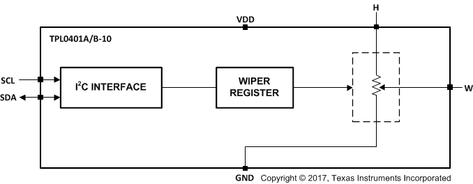
The TPL0401x-10 has a single linear-taper digital potentiometer with 128 wiper positions and an end-to-end resistance of 10 kΩ. The potentiometer can be used as a three-terminal potentiometer. The main operation of TPL0401x-10 is in voltage divider mode.
The low (L) terminal of the TPL0401x-10 is tied directly to GND. The high (H) and low (GND) terminals of TPL0401-10 are equivalent to the fixed terminals of a mechanical potentiometer. The H terminal must have a higher voltage than the low terminal (GND). The position of the wiper (W) terminal is controlled by the value in the Wiper Resistance (WR) 8-bit register. When the WR register contains all zeroes (zero-scale), the wiper terminal is closest to its L terminal. As the value of the WR register increases from all zeroes to all ones (full-scale), the wiper moves from the position closest to the GND terminal to the position closest to the H terminal. At the same time, the resistance between W and GND increases, whereas the resistance between W and H decreases.
9.2 Functional Block Diagram
9.3 Feature Description
The TPL0401x-10 device is a single-channel, linear taper digital potentiometer with 128 wiper positions. Default power up state for the TPL0401x-10 is mid code (0×40). The TPL0401x-10 has the low terminal connected to GND internally. The position of the wiper can be adjusted using an I2C interface. The TPL0401x-10 is available in a 6-pin SOT package with a specified temperature range of –40°C to +125°C. The part has a 10-kΩ end-to-end resistance and can operate with a supply voltage range of 2.7 V to 5.5 V. This kind of product is widely used in setting the voltage reference for low power DDR3 memory. The TPL0401x-10 has the low terminal internal and connected to GND.
9.4 Device Functional Modes
9.4.1 Voltage Divider Mode
The digital potentiometer generates a voltage divider when all three terminals are used. The voltage divider at wiper-to-H and wiper-to-GND is proportional to the input voltage at H to L (see Figure 11).
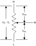 Figure 11. Equivalent Circuit for Voltage Divider Mode
For example, connecting terminal H to 5 V, the output voltage at terminal W can range from 0 V to 5 V. Equation 1 is the general equation defining the output voltage at terminal W for any valid input voltage applied to terminal H and terminal L (GND).

The voltage difference between terminal H and terminal W can also be calculated in Equation 2.

where
- D is the decimal value of the wiper code
Table 1 shows the ideal values for DPOT with end-to end resistance of 10 kΩ. The absolute values of resistance can vary significantly but the Ratio (RWL/RTOT) is extremely accurate.
The linearity values are relative linearity values (that is, linearity after zero-scale and full-scale offset errors are removed). Consider this when expecting a certain absolute accuracy because some error is introduced when the device gets close in magnitude to the offset errors.
Note that the MSB is always discarded during a write to the wiper position register. For example, if 0x80 is written to the wiper position register, a read returns 0x00. Another similar example is if 0xFF is written, then 0x7F is read.
Table 1. Resistance Values Table
| STEP | HEX | RWL (KΩ) | RHW (KΩ) | RWL/RTOT |
|---|---|---|---|---|
| 0 | 0x00 | 0.00 | 10.00 | 0.0% |
| 1 | 0x01 | 0.08 | 9.92 | 0.8% |
| 2 | 0x02 | 0.16 | 9.84 | 1.6% |
| 3 | 0x03 | 0.23 | 9.77 | 2.3% |
| 4 | 0x04 | 0.31 | 9.69 | 3.1% |
| 5 | 0x05 | 0.39 | 9.61 | 3.9% |
| 6 | 0x06 | 0.47 | 9.53 | 4.7% |
| 7 | 0x07 | 0.55 | 9.45 | 5.5% |
| 8 | 0x08 | 0.63 | 9.38 | 6.3% |
| 9 | 0x09 | 0.70 | 9.30 | 7.0% |
| 10 | 0x0A | 0.78 | 9.22 | 7.8% |
| 11 | 0x0B | 0.86 | 9.14 | 8.6% |
| 12 | 0x0C | 0.94 | 9.06 | 9.4% |
| 13 | 0x0D | 1.02 | 8.98 | 10.2% |
| 14 | 0x0E | 1.09 | 8.91 | 10.9% |
| 15 | 0x0F | 1.17 | 8.83 | 11.7% |
| 16 | 0x10 | 1.25 | 8.75 | 12.5% |
| 17 | 0x11 | 1.33 | 8.67 | 13.3% |
| 18 | 0x12 | 1.41 | 8.59 | 14.1% |
| 19 | 0x13 | 1.48 | 8.52 | 14.8% |
| 20 | 0x14 | 1.56 | 8.44 | 15.6% |
| 21 | 0x15 | 1.64 | 8.36 | 16.4% |
| 22 | 0x16 | 1.72 | 8.28 | 17.2% |
| 23 | 0x17 | 1.80 | 8.20 | 18.0% |
| 24 | 0x18 | 1.88 | 8.13 | 18.8% |
| 25 | 0x19 | 1.95 | 8.05 | 19.5% |
| 26 | 0x1A | 2.03 | 7.97 | 20.3% |
| 27 | 0x1B | 2.11 | 7.89 | 21.1% |
| 28 | 0x1C | 2.19 | 7.81 | 21.9% |
| 29 | 0x1D | 2.27 | 7.73 | 22.7% |
| 30 | 0x1E | 2.34 | 7.66 | 23.4% |
| 31 | 0x1F | 2.42 | 7.58 | 24.2% |
| 32 | 0x20 | 2.50 | 7.50 | 25.0% |
| 33 | 0x21 | 2.58 | 7.42 | 25.8% |
| 34 | 0x22 | 2.66 | 7.34 | 26.6% |
| 35 | 0x23 | 2.73 | 7.27 | 27.3% |
| 36 | 0x24 | 2.81 | 7.19 | 28.1% |
| 37 | 0x25 | 2.89 | 7.11 | 28.9% |
| 38 | 0x26 | 2.97 | 7.03 | 29.7% |
| 39 | 0x27 | 3.05 | 6.95 | 30.5% |
| 40 | 0x28 | 3.13 | 6.88 | 31.3% |
| 41 | 0x29 | 3.20 | 6.80 | 32.0% |
| 42 | 0x2A | 3.28 | 6.72 | 32.8% |
| 43 | 0x2B | 3.36 | 6.64 | 33.6% |
| 44 | 0x2C | 3.44 | 6.56 | 34.4% |
| 45 | 0x2D | 3.52 | 6.48 | 35.2% |
| 46 | 0x2E | 3.59 | 6.41 | 35.9% |
| 47 | 0x2F | 3.67 | 6.33 | 36.7% |
| 48 | 0x30 | 3.75 | 6.25 | 37.5% |
| 49 | 0x31 | 3.83 | 6.17 | 38.3% |
| 50 | 0x32 | 3.91 | 6.09 | 39.1% |
| 51 | 0x33 | 3.98 | 6.02 | 39.8% |
| 52 | 0x34 | 4.06 | 5.94 | 40.6% |
| 53 | 0x35 | 4.14 | 5.86 | 41.4% |
| 54 | 0x36 | 4.22 | 5.78 | 42.2% |
| 55 | 0x37 | 4.30 | 5.70 | 43.0% |
| 56 | 0x38 | 4.38 | 5.63 | 43.8% |
| 57 | 0x39 | 4.45 | 5.55 | 44.5% |
| 58 | 0x3A | 4.53 | 5.47 | 45.3% |
| 59 | 0x3B | 4.61 | 5.39 | 46.1% |
| 60 | 0x3C | 4.69 | 5.31 | 46.9% |
| 61 | 0x3D | 4.77 | 5.23 | 47.7% |
| 62 | 0x3E | 4.84 | 5.16 | 48.4% |
| 63 | 0x3F | 4.92 | 5.08 | 49.2% |
| 64 (POR Default) | 0x40 | 5.00 | 5.00 | 50.0% |
| 65 | 0x41 | 5.08 | 4.92 | 50.8% |
| 66 | 0x42 | 5.16 | 4.84 | 51.6% |
| 67 | 0x43 | 5.23 | 4.77 | 52.3% |
| 68 | 0x44 | 5.31 | 4.69 | 53.1% |
| 69 | 0x45 | 5.39 | 4.61 | 53.9% |
| 70 | 0x46 | 5.47 | 4.53 | 54.7% |
| 71 | 0x47 | 5.55 | 4.45 | 55.5% |
| 72 | 0x48 | 5.63 | 4.38 | 56.3% |
| 73 | 0x49 | 5.70 | 4.30 | 57.0% |
| 74 | 0x4A | 5.78 | 4.22 | 57.8% |
| 75 | 0x4B | 5.86 | 4.14 | 58.6% |
| 76 | 0x4C | 5.94 | 4.06 | 59.4% |
| 77 | 0x4D | 6.02 | 3.98 | 60.2% |
| 78 | 0x4E | 6.09 | 3.91 | 60.9% |
| 79 | 0x4F | 6.17 | 3.83 | 61.7% |
| 80 | 0x50 | 6.25 | 3.75 | 62.5% |
| 81 | 0x51 | 6.33 | 3.67 | 63.3% |
| 82 | 0x52 | 6.41 | 3.59 | 64.1% |
| 83 | 0x53 | 6.48 | 3.52 | 64.8% |
| 84 | 0x54 | 6.56 | 3.44 | 65.6% |
| 85 | 0x55 | 6.64 | 3.36 | 66.4% |
| 86 | 0x56 | 6.72 | 3.28 | 67.2% |
| 87 | 0x57 | 6.80 | 3.20 | 68.0% |
| 88 | 0x58 | 6.88 | 3.13 | 68.8% |
| 89 | 0x59 | 6.95 | 3.05 | 69.5% |
| 90 | 0x5A | 7.03 | 2.97 | 70.3% |
| 91 | 0x5B | 7.11 | 2.89 | 71.1% |
| 92 | 0x5C | 7.19 | 2.81 | 71.9% |
| 93 | 0x5D | 7.27 | 2.73 | 72.7% |
| 94 | 0x5E | 7.34 | 2.66 | 73.4% |
| 95 | 0x5F | 7.42 | 2.58 | 74.2% |
| 96 | 0x60 | 7.50 | 2.50 | 75.0% |
| 97 | 0x61 | 7.58 | 2.42 | 75.8% |
| 98 | 0x62 | 7.66 | 2.34 | 76.6% |
| 99 | 0x63 | 7.73 | 2.27 | 77.3% |
| 100 | 0x64 | 7.81 | 2.19 | 78.1% |
| 101 | 0x65 | 7.89 | 2.11 | 78.9% |
| 102 | 0x66 | 7.97 | 2.03 | 79.7% |
| 103 | 0x67 | 8.05 | 1.95 | 80.5% |
| 104 | 0x68 | 8.13 | 1.88 | 81.3% |
| 105 | 0x69 | 8.20 | 1.80 | 82.0% |
| 106 | 0x6A | 8.28 | 1.72 | 82.8% |
| 107 | 0x6B | 8.36 | 1.64 | 83.6% |
| 108 | 0x6C | 8.44 | 1.56 | 84.4% |
| 109 | 0x6D | 8.52 | 1.48 | 85.2% |
| 110 | 0x6E | 8.59 | 1.41 | 85.9% |
| 111 | 0x6F | 8.67 | 1.33 | 86.7% |
| 112 | 0x70 | 8.75 | 1.25 | 87.5% |
| 113 | 0x71 | 8.83 | 1.17 | 88.3% |
| 114 | 0x72 | 8.91 | 1.09 | 89.1% |
| 115 | 0x73 | 8.98 | 1.02 | 89.8% |
| 116 | 0x74 | 9.06 | 0.94 | 90.6% |
| 117 | 0x75 | 9.14 | 0.86 | 91.4% |
| 118 | 0x76 | 9.22 | 0.78 | 92.2% |
| 119 | 0x77 | 9.30 | 0.70 | 93.0% |
| 120 | 0x78 | 9.38 | 0.63 | 93.8% |
| 121 | 0x79 | 9.45 | 0.55 | 94.5% |
| 122 | 0x7A | 9.53 | 0.47 | 95.3% |
| 123 | 0x7B | 9.61 | 0.39 | 96.1% |
| 124 | 0x7C | 9.69 | 0.31 | 96.9% |
| 125 | 0x7D | 9.77 | 0.23 | 97.7% |
| 126 | 0x7E | 9.84 | 0.16 | 98.4% |
| 127 | 0x7F | 9.92 | 0.08 | 99.2% |
9.5 Programming
9.5.1 I2C General Operation and Overview
9.5.1.1 START and STOP Conditions
I2C communication with this device is initiated by the master sending a START condition and terminated by the master sending a STOP condition. A high-to-low transition on the SDA line while the SCL is high defines a START condition. A low-to-high transition on the SDA line while the SCL is high defines a STOP condition. See Figure 12.
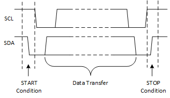 Figure 12. Definition of START and STOP Conditions
9.5.1.2 Data Validity and Byte Formation
One data bit is transferred during each clock pulse of the SCL. One byte is comprised of eight bits on the SDA line. See Figure 13. A byte may either be a device address, register address, or data written to or read from a slave.
Data is transferred Most Significant Bit (MSB) first. Any number of data bytes can be transferred from the master to slave between the START and STOP conditions. Data on the SDA line must remain stable during the high phase of the clock period, as changes in the data line when the SCL is high are interpreted as control commands (START or STOP).
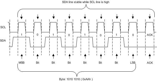 Figure 13. Definition of Byte Formation
9.5.1.3 Acknowledge (ACK) and Not Acknowledge (NACK)
Each byte is followed by one ACK bit from the receiver. The ACK bit allows the receiver to communicate to the transmitter that the byte was successfully received and another byte may be sent.
The transmitter must release the SDA line before the receiver can send the ACK bit. To send an ACK bit, the receiver shall pull down the SDA line during the low phase of the ACK/NACK-related clock period (period 9), so that the SDA line is stable low during the high phase of the ACK/NACK-related clock period. Consider setup and hold times. Figure 14 shows an example use of ACK.
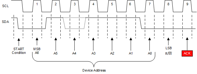 Figure 14. Example Use of ACK
When the SDA line remains high during the ACK/NACK-related clock period, this is a NACK signal. There are several conditions that lead to the generation of a NACK:
- The receiver is unable to receive or transmit because it is performing some real-time function and is not ready to start communication with the master.
- During the transfer, the receiver gets data or commands that it does not understand.
- During the transfer, the receiver cannot receive any more data bytes.
- A master-receiver is done reading data and indicates this to the slave through a NACK.
Figure 15 shows an example use of NACK.
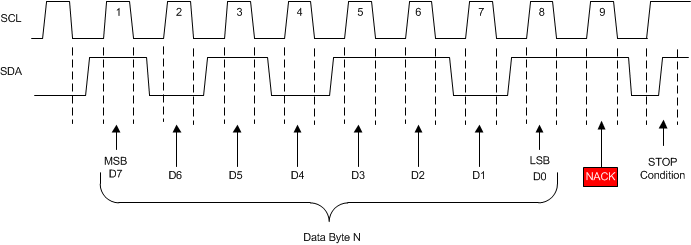 Figure 15. Example Use of NACK
9.5.1.4 Repeated Start
A repeated START condition may be used in place of a complete STOP condition follow by another START condition when performing a read function. The advantage of this is that the I2C bus does not become available after the stop and therefore prevents other devices from grabbing the bus between transfers.
9.5.2 Programing with I2C
9.5.2.1 Write Operation
To write on the I2C bus, the master sends a START condition on the bus with the address of the slave, as well as the last bit (the R/W bit) set to 0, which signifies a write. After the slave responds with an acknowledge, the master then sends the register address of the register to which it wishes to write. The slave acknowledges again, letting the master know that it is ready. After this, the master starts sending the register data to the slave until the master has sent all the data necessary (which is sometimes only a single byte), and the master terminates the transmission with a STOP condition. See Figure 16.
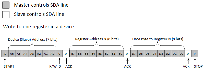 Figure 16. Write Operation
9.5.2.2 Read Operation
Reading from a slave is very similar to writing, but requires some additional steps. in order to read from a slave, the master must first instruct the slave which register it wishes to read from. This is done by the master starting off the transmission in a similar fashion as the write, by sending the address with the R/W bit equal to 0 (signifying a write), followed by the register address it wishes to read from. When the slave acknowledges this register address, the master sends a START condition again, followed by the slave address with the R/W bit set to 1 (Signifying a read). This time, the slave acknowledges the read request, and the master releases the SDA bus but continues supplying the clock to the slave. During this part of the transaction, the master becomes the master-receiver, and the slave becomes the slave-transmission.
The master continues to send out the clock pulses, for each byte of data that it wishes to receive. At the end of every byte of data, the master sends an ACK to the slave, letting the slave know that it is ready for more data. When the master has received the number of bytes it was expecting (or needs to stop communication), it sends a NACK, signaling to the slave to halt communications and release the bus. The master follows this up with a STOP condition. Figure 17 shows the read operation from one register.
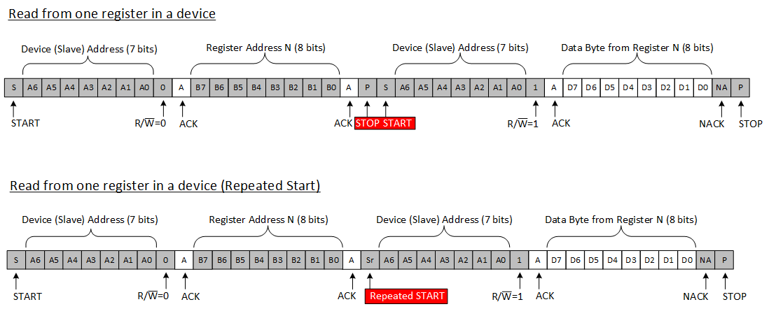 Figure 17. Read Operation from One Register
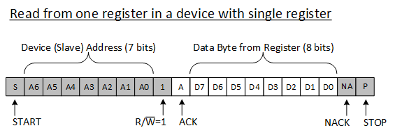 Figure 18. Short Read Operation
The TPL0401x-10 has 1 register, and it is not a requirement that the register address be sent before a read. A shorter read allows the user to simply send a read request to the device address as shown in Figure 18.
9.6 Register Maps
9.6.1 Slave Address
Table 1 and Table 2 show the TPL0401A-10 and TPL0401B-10 bit address repectively.
Table 1. TPL0401A-10 Bit Address
| BIT 7 (MSB) |
BIT 6 | BIT 5 | BIT 4 | BIT 3 | BIT 2 | BIT 1 | BIT 0 (LSB) |
| 0 | 1 | 0 | 1 | 1 | 1 | 0 | R/W |
Table 2. TPL0401B-10 Bit Address
| BIT 7 (MSB) |
BIT 6 | BIT 5 | BIT 4 | BIT 3 | BIT 2 | BIT 1 | BIT 0 (LSB) |
| 0 | 1 | 1 | 1 | 1 | 1 | 0 | R/W |
9.6.2 Register Address
Following the successful acknowledgment of the address byte, the bus master sends a command byte as shown in Figure 19, which is stored in the Control Register in the TPL0401x-10. The TPL0401x-10 has only 1 register, but requires the command byte be sent during communication.
 Figure 19. Register Address Byte
Table 2 shows the TPL0401x-10 register address byte.
Table 2. Register Address Byte
| REGISTER ADDRESS BITS | REGISTER ADDRESS (HEX) |
REGISTER | PROTOCOL | POWER-UP DEFAULT |
|||||||
|---|---|---|---|---|---|---|---|---|---|---|---|
| B7 | B6 | B5 | B4 | B3 | B2 | B1 | B0 | ||||
| 0 | 0 | 0 | 0 | 0 | 0 | 0 | 0 | 0x00 | Wiper Position | Read/Write byte | 0100 0000 (0×40) |
See Table 1 for more information on the wiper position register values. Note that the MSB is always discarded during a write to the wiper position register. For example, if 0x80 is written to the wiper position register, a read returns 0x00. Another similar example is if 0xFF is written, then 0x7F is read.