SNAS659B June 2015 – September 2018 TPL5111
PRODUCTION DATA.
- 1 Features
- 2 Applications
- 3 Description
- 4 Revision History
- 5 Pin Configuration and Functions
- 6 Specifications
- 7 Detailed Description
- 8 Application and Implementation
- 9 Power Supply Recommendations
- 10Layout
- 11Device and Documentation Support
- 12Mechanical, Packaging, and Orderable Information
Package Options
Mechanical Data (Package|Pins)
- DDC|6
Thermal pad, mechanical data (Package|Pins)
Orderable Information
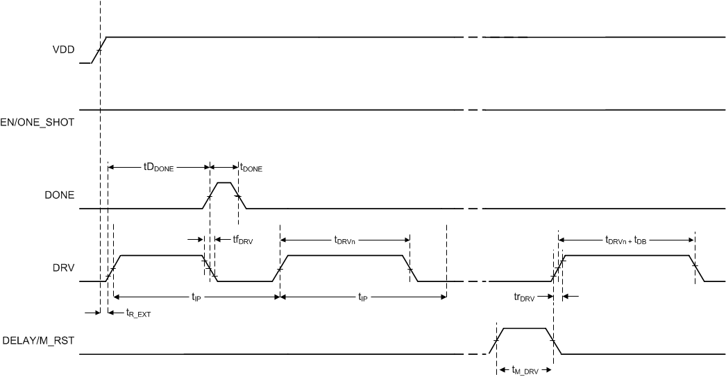
6.6 Timing Requirements
| MIN(3) | NOM(4) | MAX(3) | UNIT | ||||
|---|---|---|---|---|---|---|---|
| trDRVn | Rise Time DRVn(2) | Capacitive load 50 pF | 50 | ns | |||
| tfDRVn | Fall Time DRVn(2) | Capacitive load 50 pF | 50 | ns | |||
| tDDONE | DONE to DRVn delay | Minimum delay(1) | 100 | ns | |||
| Maximum delay (1) | tDRVn | ||||||
| tM_DRV | Valid manual MOSFET Power ON | Observation time 30 ms | 20 | ms | |||
| tDB | De-bounce manual MOSFET Power ON | 20 | ms | ||||
(1) From DRVn rising edge.
(2) This parameter is specified by design and/or characterization and is not tested in production.
(3) Limits are specified by testing, design, or statistical analysis at 25°C. Limits over the operating temperature range are specified through correlations using statistical quality control (SQC) method.
(4) Typical values represent the most likely parametric norm as determined at the time of characterization. Actual typical values may vary over time and will also depend on the application and configuration. The typical values are not tested and are not specified on shipped production material.
 Figure 1. TPL5111 Timing