SLRS066D January 2014 – March 2016 TPL7407L
PRODUCTION DATA.
- 1 Features
- 2 Applications
- 3 Description
- 4 Revision History
- 5 Pin Configuration and Functions
- 6 Specifications
- 7 Detailed Description
- 8 Application and Implementation
- 9 Power Supply Recommendations
- 10Layout
- 11Device and Documentation Support
- 12Mechanical, Packaging, and Orderable Information
Package Options
Mechanical Data (Package|Pins)
Thermal pad, mechanical data (Package|Pins)
Orderable Information
7 Detailed Description
7.1 Overview
This device has proven ubiquity and versatility across a wide range of applications. This is due to it's integration of 7 low side NMOS transistors that are capable of sinking up to 600mA and wide GPIO range capability.
The TPL7407L comprises seven high voltage, high current NMOS transistors tied to a common ground driven by internal level shifting and gate drive circuitry. The TPL7407L offers solutions to many interface needs, including solenoids, relays, lamps, small motors, and LEDs. Applications requiring sink currents beyond the capability of a single output may be accommodated by paralleling the outputs.
The TPL7407L also enables pin to pin replacement with legacy 7 channel darlington pair implementations
This device can operate over a wide temperature range (–40°C to 125°C).
7.2 Functional Block Diagram

7.3 Feature Description
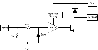
Each channel of TPL7407L consists of high power low side NMOS transistors driven by level shifting and gate driving circuitry. The gate drivers allow for high output current drive with a very low input voltage, essentially equating to operability with low GPIO voltages.
In order to enable floating inputs a 1MΩ pull-down resistor exists on each channel. Another 50-kΩ resistor exists between the input and gate driving circuitry. This exists to limit the input current whenever there is an over voltage and the internal Zener clamps. It also interacts with the inherent capacitance of the gate driving circuitry to behave as an RC snubber to help prevent spurious switching in noisy environment.
In order to power the gate driving circuitry an LDO exists. See Power Supply Recommendations for further detail on this circuitry.
The diodes connected between the output and COM pin is used to surpress kick-back voltage from an inductive load that is excited when the NMOS drivers are turned off (stop sinking) and the stored energy in the coils causes a reverse current to flow into the coil supply.
7.4 Device Functional Modes
7.4.1 Inductive Load Drive
When the COM pin is tied to the coil supply voltage, TPL7407L is able to drive inductive loads and supress the kick-back voltage via the internal free wheeling diodes.
7.4.2 Resistive Load Drive
When driving a resistive load, a pull-up resistor is needed in order for TPL7407L to sink current and for there to be a logic high level. The COM pin should be supplied ≥8.5V for full functionality.