SLVSDO6C August   2017  – June 2019 TPS1H000-Q1

PRODUCTION DATA.  

  1. Features
  2. Applications
  3. Description
    1.     Device Images
      1.      Typical Block Diagram
      2.      Current-Limit Protection in Auto-Retry Mode
  4. Revision History
  5. Pin Configuration and Functions
    1.     Pin Functions
  6. Specifications
    1. 6.1 Absolute Maximum Ratings
    2. 6.2 ESD Ratings
    3. 6.3 Recommended Operating Conditions
    4. 6.4 Thermal Information
    5. 6.5 Electrical Characteristics
    6. 6.6 Switching Characteristics
    7. 6.7 Typical Characteristics
  7. Detailed Description
    1. 7.1 Overview
    2. 7.2 Functional Block Diagram
    3. 7.3 Feature Description
      1. 7.3.1 Current Limit
      2. 7.3.2 DELAY Pin Configuration
        1. 7.3.2.1 Holding Mode
        2. 7.3.2.2 Latch-Off Mode
        3. 7.3.2.3 Auto-Retry Mode
      3. 7.3.3 Standalone Operation
      4. 7.3.4 Fault Truth Table
      5. 7.3.5 Full Diagnostics
        1. 7.3.5.1 Short-to-GND and Overload Detection
        2. 7.3.5.2 Open-Load Detection
          1. 7.3.5.2.1 Output On
          2. 7.3.5.2.2 Output Off
        3. 7.3.5.3 Short-to-Battery Detection
        4. 7.3.5.4 Thermal Fault Detection
          1. 7.3.5.4.1 Thermal Shutdown
          2. 7.3.5.4.2 Thermal Swing
          3. 7.3.5.4.3 Fault Report Holding
      6. 7.3.6 Full Protections
        1. 7.3.6.1 UVLO Protection
        2. 7.3.6.2 Inductive Load Switching Off Clamp
        3. 7.3.6.3 Loss-of-GND Protection
        4. 7.3.6.4 Loss-of-Power-Supply Protection
        5. 7.3.6.5 Reverse-Current Protection
        6. 7.3.6.6 MCU I/O Protection
    4. 7.4 Device Functional Modes
      1. 7.4.1 Working Modes
        1. 7.4.1.1 Normal Mode
        2. 7.4.1.2 Standby Mode
        3. 7.4.1.3 Standby Mode With Diagnostics
  8. Application and Implementation
    1. 8.1 Application Information
    2. 8.2 Typical Application
      1. 8.2.1 Design Requirements
      2. 8.2.2 Detailed Design Procedure
      3. 8.2.3 Application Curves
  9. Power Supply Recommendations
  10. 10Layout
    1. 10.1 Layout Guidelines
    2. 10.2 Layout Example
  11. 11Device and Documentation Support
    1. 11.1 Receiving Notification of Documentation Updates
    2. 11.2 Community Resources
    3. 11.3 Trademarks
    4. 11.4 Electrostatic Discharge Caution
    5. 11.5 Glossary
  12. 12Mechanical, Packaging, and Orderable Information

Package Options

Mechanical Data (Package|Pins)
Thermal pad, mechanical data (Package|Pins)
Orderable Information

Switching Characteristics

PARAMETER TEST CONDITIONS MIN NOM MAX UNIT
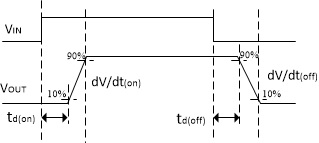
td(on) Turnon delay time, IN rising edge to 10% of VOUT VVS = 13.5 V, VDIAG_EN = 5 V, IOUT = 0.1 A 20 50 90 µs
td(off) Turnoff delay time, IN falling edge to 90% of VOUT VVS = 13.5 V, VDIAG_EN = 5 V, IOUT = 0.1 A 20 50 90 µs
dV/dt(on) Slew rate on, VOUT from 10% to 90% VVS = 13.5 V, VDIAG_EN = 5 V, IOUT = 0.1 A 0.1 0.6 V/µs
dV/dt(off) Slew rate off, VOUTfrom 90% to 10% VVS = 13.5 V, VDIAG_EN = 5 V, IOUT = 0.1 A 0.3 0.9 V/µs
TPS1H000-Q1 Slew-Rate.gifFigure 1. Output Delay Characteristics
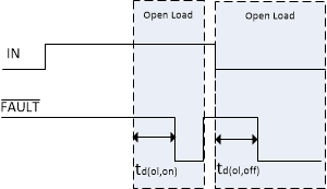
TPS1H000-Q1 Open-Load-Blanking-Time-Characteristics.gifFigure 2. Open-Load Blanking-Time Characteristic