SLVSAX6H October 2011 – December 2015 TPS2002C , TPS2003C , TPS2052C , TPS2060C , TPS2062C , TPS2062C-2 , TPS2064C , TPS2064C-2 , TPS2066C , TPS2066C-2
PRODUCTION DATA.
- 1 Features
- 2 Applications
- 3 Description
- 4 Revision History
- 5 Device Comparison Table
- 6 Pin Configuration and Functions
- 7 Specifications
- 8 Parameter Measurement Information
- 9 Detailed Description
- 10Application and Implementation
- 11Power Supply Recommendations
- 12Layout
- 13Device and Documentation Support
- 14Mechanical, Packaging, and Orderable Information
Package Options
Mechanical Data (Package|Pins)
Thermal pad, mechanical data (Package|Pins)
- DGN|8
Orderable Information
9 Detailed Description
9.1 Overview
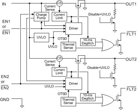
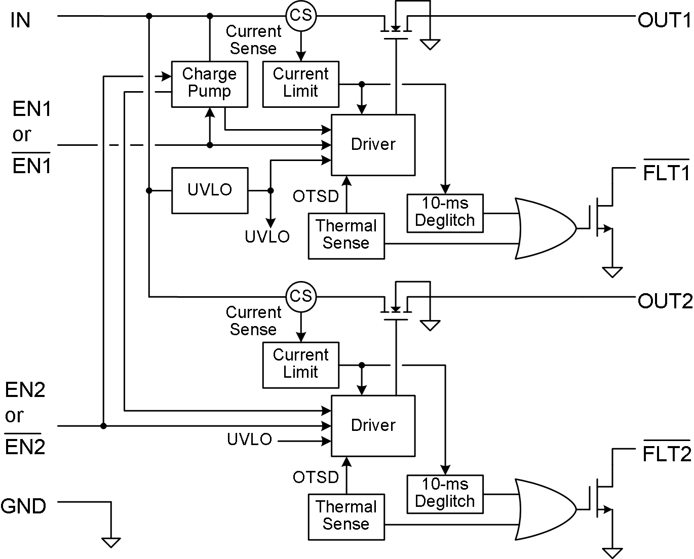
The TPS20xxC and TPS20xxC-2 are dual current-limited, power-distribution switches providing between 0.5 A and 2 A of continuous load current in 5-V circuits. These parts use N-channel MOSFETs for low resistance, maintaining output voltage load regulation. They are designed for applications where short circuits or heavy capacitive loads are encountered. Device features include UVLO, ON/OFF control (Enable), reverse blocking when disabled, output discharge when TPS20xxC disabled, overcurrent protection, overtemperature protection, and deglitched fault reporting. They are pin for pin with existing TI Switch Portfolio.
9.2 Functional Block Diagram


9.3 Feature Description
9.3.1 Undervoltage Lockout (UVLO)
The undervoltage lockout (UVLO) circuit disables the power switch when the input voltage is below the UVLO threshold. Built-in hysteresis prevents unwanted ON/OFF cycling due to input voltage drop from large current surges. FLTx is high impedance when the TPS20xxC and TPS20xxC-2 dual are in UVLO.
9.3.2 Enable (ENx or ENx)
The logic input of ENx or ENx disables all of the internal circuitry while maintaining the power switch OFF. The supply current of the device can be reduced to less than 1 µA when both switches are disabled. A logic low input on ENx or a logic high input on ENx enables the driver, control circuits, and power switch of corresponding channel.
The ENx or ENx input voltage is compatible with both TTL and CMOS logic levels. The FLTx is immediately cleared and the output discharge circuit is enabled when the device is disabled.
9.3.3 Deglitched Fault Reporting
FLTx is an open-drain output that asserts (active low) during an overcurrent or overtemperature condition on each corresponding channel. The FLTx output remains asserted until the fault condition is removed or the channel is disabled. The TPS20xxC and TPS20xxC-2 dual eliminates false FLTx reporting by using internal delay circuitry after entering or leaving an overcurrent condition. The deglitch time is typically 10 ms. This ensures that FLTx is not accidentally asserted under overcurrent conditions with a short time, such as starting into a heavy capacitive load. Overtemperature conditions are not deglitched. The FLTx pin is high impedance when the device is disabled and in undervoltage lockout (UVLO). The fault circuits are independent so that another channel continues to operate when one channel is in a fault condition.
9.3.4 Overcurrent Protection
The TPS20xxC and TPS20xxC-2 dual responds to overloads by limiting each channel output current to the static IOS levels shown in Electrical Characteristics: TJ = TA = 25°C. When an overload condition is present, the device maintains a constant current (IOS) and reduces the output voltage accordingly, with the output voltage falling to (IOS × RSHORT). Three possible overload conditions can occur. In the first condition, the output has been shorted before the device is enabled or before voltage is applied to IN. The device senses over-current and immediately switches into a constant-current output. In the second condition, a short or an overload occurs while the device is enabled. At the instant a short-circuit occurs, high currents may flow for several microseconds (tIOS) before the current-limit circuit reacts. The device operates in constant-current mode after the current-limit circuit has responded. In the third condition, the load is increased gradually beyond the recommended operating current. The current is permitted to rise until the current-limit threshold is reached. The devices are capable of delivering current up to the current-limit threshold without damage. Once the threshold is reached, the device switches into constant-current mode. For all of the above three conditions, the device may begin thermal cycling if the overcurrent condition persists.
9.3.5 Overtemperature Protection
The TPS20xxC and TPS20xxC-2 dual includes per channel overtemperature protection circuitry, which activates at 135°C (minimum) junction temperature while in current limit. There is an overall thermal shutdown of 155°C (minimum) junction temperature when the TPS20xxC and TPS20xxC-2 dual are not in current limit. The device remains off until the junction temperature cools 20°C and then restarts. Thermal shutdown may occur during an overload due to the relatively large power dissipation [(VIN – VOUT) × IOS] driving the junction temperature up. The power switch cycles on and off until the fault is removed. This topology allows one channel to continue normal operation even if the other channel is in an overtemperature condition.
9.3.6 Softstart, Reverse Blocking and Discharge Output
The power MOSFET driver incorporates circuitry that controls the rise and fall times of the output voltage to limit large current and voltage surges on the input supply, and provides built-in soft-start functionality.
The TPS20xxC and TPS20xxC-2 dual power switch will block current from OUT to IN when turned off by the UVLO or disabled.
The TPS20xxC dual includes an output discharge function on each channel. A 470 Ω (typical) discharge resistor will dissipate stored charge and leakage current on OUTx when the device is in UVLO or disabled. However as this circuit is biased from IN, the output discharge will not be active when IN voltage is close to 0 V.
The TPS20xxC-2 does not have this function. The output is be controlled by an external loadings when the device is in ULVO or disabled.
9.4 Device Functional Modes
There are no other functional modes.