SBVS124A November 2008 – May 2016 TPS2115A-Q1
PRODUCTION DATA.
- 1 Features
- 2 Applications
- 3 Description
- 4 Revision History
- 5 Pin Configuration and Functions
- 6 Specifications
- 7 Parameter Measurement Information
- 8 Detailed Description
- 9 Application and Information
- 10Power Supply Recommendations
- 11Layout
- 12Device and Documentation Support
- 13Mechanical, Packaging, and Orderable Information
Package Options
Mechanical Data (Package|Pins)
- PW|8
Thermal pad, mechanical data (Package|Pins)
Orderable Information
1 Features
- Qualified for Automotive Applications
- AEC-Q100 Qualified With the Following Results:
- Device Temperature Grade 3: –40°C to 85°C Ambient Operating Temperature Range
- Device HBM ESD Classification Level 2
- Device CDM ESD Classification Level C4A
- Two-Input One-Output Power Multiplexer With Low rDS(on) Switch...84 mΩ (Typical)
- Reverse and Cross-Conduction Blocking
- Wide Operating Voltage Range...2.8 V to 5.5 V
- Low Standby Current...0.5 μA (Typical)
- Low Operating Current...55 μA (Typical)
- Adjustable Current Limit
- Controlled Output-Voltage Transition Times Limit Inrush Current and Minimize Output Voltage Hold-Up Capacitance
- CMOS- and TTL-Compatible Control Inputs
- Manual and Auto-Switching Operating Modes
- Thermal Shutdown
- Available in TSSOP-8 (PW) Package
2 Applications
3 Description
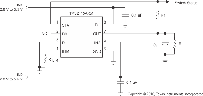
The TPS2115A-Q1 power multiplexer enables seamless transition between two power supplies, such as a two supply rails or a battery and AC to DC wall adapter. Each supply operates at 2.8 V to 5.5 V and the output can deliver up to 1 A. The TPS2115A-Q1 device includes extensive protection circuitry including user-programmable current limiting, thermal protection, inrush current control, seamless supply transition, cross-conduction blocking, and reverse-conduction blocking. These features greatly simplify designing power multiplexer applications.
Device Information(1)
| PART NUMBER | PACKAGE | BODY SIZE (NOM) |
|---|---|---|
| TPS2115A-Q1 | TSSOP (8) | 4.40 mm × 3.0 mm |
- For all available packages, see the orderable addendum at the end of the data sheet.
Typical Application
