SBVS124A November 2008 – May 2016 TPS2115A-Q1
PRODUCTION DATA.
- 1 Features
- 2 Applications
- 3 Description
- 4 Revision History
- 5 Pin Configuration and Functions
- 6 Specifications
- 7 Parameter Measurement Information
- 8 Detailed Description
- 9 Application and Information
- 10Power Supply Recommendations
- 11Layout
- 12Device and Documentation Support
- 13Mechanical, Packaging, and Orderable Information
Package Options
Mechanical Data (Package|Pins)
- PW|8
Thermal pad, mechanical data (Package|Pins)
Orderable Information
11 Layout
11.1 Layout Guidelines
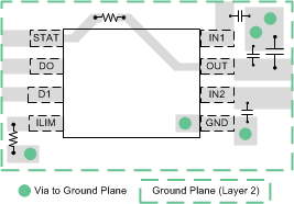
- For the first supply input (IN1), place the 0.1-μF bypass capacitor between the IN1 and GND as close as possible ensuring a low-impedance trace.
- For the second supply input (IN2), place the 0.1-μF bypass capacitor between the IN2 and GND as close as possible ensuring a low-impedance trace.
- Place a high-value capacitor and a 0.1-μF bypass capacitor between OUT and GND. The recommendation is to use the high-value capacitor when expecting large-load transients on the output. This trace should be low-impedance to the load.
- Place the resistor used to set the current limit between ILIM and GND. Make sure the traces routing the RILIM resistor to the device are as short as possible to reduce parasitic effects on the current limit accuracy.
11.2 Layout Example
 Figure 24. TPS2115A-Q1 Layout Example