SLVSGU5A April 2022 – July 2022 TPS22811
PRODUCTION DATA
- 1 Features
- 2 Applications
- 3 Description
- 4 Revision History
- 5 Pin Configuration and Functions
- 6 Specifications
-
7 Detailed Description
- 7.1 Overview
- 7.2 Functional Block Diagram
- 7.3
Feature Description
- 7.3.1 Undervoltage Lockout (UVLO and UVP)
- 7.3.2 Overvoltage Lockout (OVLO)
- 7.3.3 Inrush Current, Overcurrent, and Short-Circuit Protection
- 7.3.4 Analog Load Current Monitor
- 7.3.5 Overtemperature Protection (OTP)
- 7.3.6 Fault Response
- 7.3.7 Power-Good Indication (PG)
- 7.3.8 Quick Output Discharge (QOD)
- 7.4 Device Functional Modes
- 8 Application and Implementation
- 9 Power Supply Recommendations
- 10Layout
- 11Device and Documentation Support
- 12Mechanical, Packaging, and Orderable Information
Package Options
Mechanical Data (Package|Pins)
- RPW|10
Thermal pad, mechanical data (Package|Pins)
Orderable Information
7.3.2 Overvoltage Lockout (OVLO)
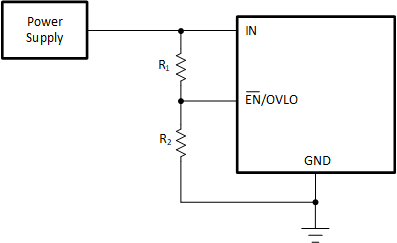
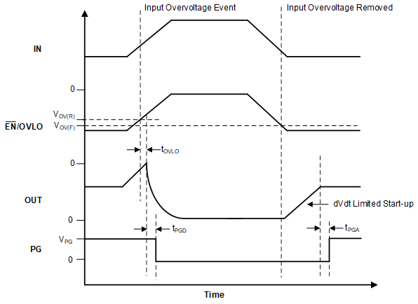
The TPS22811x allows the user to implement overvoltage lockout to protect the load from input overvoltage conditions. The OVLO comparator on the EN/OVLO pin allows the overvoltage protection threshold to be adjusted to a user defined value. After the voltage at the EN/OVLO pin crosses the OVLO rising threshold VOV(R), the device turns off the power to the output. Thereafter, the devices wait for the voltage at the EN/OVLO pin to fall below the OVLO falling threshold VOV(F) before the output power is turned ON again. The rising and falling thresholds are slightly different to provide hysterisis. Figure 7-2 and Equation 2 show how a resistor divider can be used to set the OVLO set point for a given voltage supply.
 Figure 7-2 Adjustable Overvoltage
Protection
 Figure 7-3 TPS22811x Overvoltage Lockout
and Recovery