SLVS749C November 2008 – January 2015 TPS22921 , TPS22922
UNLESS OTHERWISE NOTED, this document contains PRODUCTION DATA.
- 1 Features
- 2 Applications
- 3 Description
- 4 Typical Application
- 5 Revision History
- 6 Device Comparison Table
- 7 Pin Configuration and Functions
-
8 Specifications
- 8.1 Absolute Maximum Ratings
- 8.2 ESD Ratings
- 8.3 Recommended Operating Conditions
- 8.4 Thermal Information
- 8.5 Electrical Characteristics
- 8.6 Switching Characteristics: VIN = 0.9 V
- 8.7 Switching Characteristics: VIN = 1 V
- 8.8 Switching Characteristics: VIN = 1.1 V
- 8.9 Switching Characteristics: VIN = 1.2 V
- 8.10 Switching Characteristics: VIN = 1.8 V
- 8.11 Switching Characteristics: VIN = 2.5 V
- 8.12 Switching Characteristics: VIN = 3 V
- 8.13 Switching Characteristics: VIN = 3.6 V
- 8.14
Typical Characteristics
- 8.14.1 Typical DC Characteristics
- 8.14.2 Typical AC Characteristics (TPS22921)
- 8.14.3 Typical AC Characteristics (TPS22922)
- 8.14.4 Typical AC Characteristics (TPS22922B)
- 8.14.5 Typical AC Characteristics (TPS22921 and TPS22922)
- 8.14.6 Typical AC Characteristics (TPS22921)
- 8.14.7 Typical AC Characteristics (TPS22922)
- 8.14.8 Typical AC Characteristics (TPS22922B)
- 9 Parameter Measurement Information
- 10Detailed Description
- 11Application and Implementation
- 12Power Supply Recommendations
- 13Layout
- 14Device and Documentation Support
- 15Mechanical, Packaging, and Orderable Information
Package Options
Mechanical Data (Package|Pins)
Thermal pad, mechanical data (Package|Pins)
Orderable Information
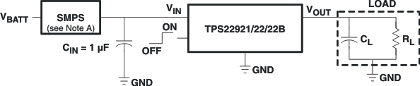
11 Application and Implementation
NOTE
Information in the following applications sections is not part of the TI component specification, and TI does not warrant its accuracy or completeness. TI’s customers are responsible for determining suitability of components for their purposes. Customers should validate and test their design implementation to confirm system functionality.
11.1 Application Information
11.1.1 Input Capacitor (Optional)
To limit the voltage drop on the input supply caused by transient inrush currents when the switch turns on into a discharged load capacitor, a capacitor must be placed between VIN and GND. A 1-μF ceramic capacitor, CIN, placed close to the pins is usually sufficient. Higher values of CIN can be used to further reduce the voltage drop during higher current application. When switching a heavy load, TI recommends using an input capacitor about 10 or more times higher than the output capacitor in order to avoid any supply drop.
11.1.2 Output Capacitor (Optional)
Because of the integral body diode in the PMOS switch, a CIN greater than CL is highly recommended. A CL greater than CIN can cause VOUT to exceed VIN when the system supply is removed. This could result in current flow through the body diode from VOUT to VIN.
11.2 Typical Application
11.2.1 Design Requirements
Table 2. Design Parameters
| DESIGN PARAMETER | EXAMPLE VALUE |
|---|---|
| VIN | 1.8 V |
| CL | 4.7 µF |
| Load current | 2 A |
| Ambient Temperature | 25 °C |
| Maximum inrush current | 200 mA |
11.2.2 Detailed Design Procedure
11.2.2.1 Managing Inrush Current
When the switch is enabled, the output capacitors must be charged up from 0 V to the set value (1.8 V in this example). This charge arrives in the form of inrush current. Inrush current can be calculated using the following equation:

where
- CL = Output capacitance
- dVOUT = Output voltage
- dt = Rise time
The TPS22921/2/2B offers a controlled rise time for minimizing inrush current. This device can be selected based upon the minimum acceptable rise time which can be calculated using the design requirements and the inrush current equation. An output capacitance of 4.7 µF will be used because the amount of inrush current increases with output capacitance:
where
- dt = 42.3 µs
To ensure an inrush current of less than 200 mA, a device with a rise time greater than 42.3 µs must be used. The TPS22922B has a typical rise time of 200 µs at 1.8 V which meets the above design requirements. The TPS22921/2 has a faster rise time of 30 µs at 1.8 V, and this would result in an inrush current larger than desired.
11.2.2.2 VIN to VOUT Voltage Drop
The voltage drop from VIN to VOUT is determined by the ON-resistance of the device and the load current. RON can be found in Electrical Characteristics and is dependent on temperature. When the value of RON is found, the following equation can be used to calculate the voltage drop across the device:
where
- ΔV = Voltage drop across the device
- ILOAD = Load current
- RON = ON-resistance of the device
At VIN = 1.8 V, the TPS22921/2/2B has an RON value of 33 mΩ. Using this value and the defined load current, the above equation can be evaluated:
where
- ΔV = 66 mV
Therefore, the voltage drop across the device will be 66 mV.
11.2.3 Application Curve
Figure 54 shows the expected voltage drop across the device for different load currents and input voltages.
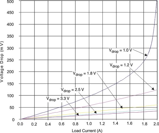 Figure 54. Voltage Drop vs Load Current