SLVSBL3D November 2012 – July 2021
PRODUCTION DATA
- 1 Features
- 2 Applications
- 3 Description
- 4 Revision History
- 5 Specifications
- 6 Pin Configuration and Functions
- 7 Parameter Measurement Information
- 8 Detailed Description
- 9 Application and Implementation
- 10Power Supply Recommendations
- 11Layout
- 12Device and Documentation Support
- 13Mechanical, Packaging, and Orderable Information
Package Options
Refer to the PDF data sheet for device specific package drawings
Mechanical Data (Package|Pins)
- YZV|4
Thermal pad, mechanical data (Package|Pins)
Orderable Information
11.3 Thermal Considerations
The maximum IC junction temperature should be restricted to 125°C under normal operating conditions. To calculate the maximum allowable dissipation, PD(max) for a given output current and ambient temperature, use the following equation as a guideline:
Equation 1. 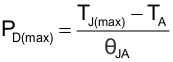
where
- PD(max) = maximum allowable power dissipation
- TJ(max) = maximum allowable junction temperature (125°C for the TPS22930)
- TA = ambient temperature of the device
- ΘJA = junction to air thermal impedance. See Thermal Information table. This parameter is highly dependent upon board layout.
The power dissipated by the device depends on the RON of the device at a given VIN. To calculate the amount of power being dissipated by the device, use the following equation:
Equation 2. 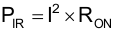
where
- PIR = power dissipated by the device
- I = load current in amperes
- RON = resistance of the device in Ohms at a given VIN (see Electrical Characteristics table)
The result from Equation 2 should always be less than or equal to the result from Equation 1.