SLVS832D November 2008 – July 2014 TPS22941 , TPS22942 , TPS22943 , TPS22944 , TPS22945
PRODUCTION DATA.
- 1 Features
- 2 Applications
- 3 Description
- 4 Revision History
- 5 Device Comparison Table
- 6 Pin Configuration and Functions
- 7 Specifications
- 8 Detailed Description
- 9 Application and Implementation
- 10Power Supply Recommendations
- 11Layout
- 12Device and Documentation Support
- 13Mechanical, Packaging, and Orderable Information
Package Options
Mechanical Data (Package|Pins)
- DCK|5
Thermal pad, mechanical data (Package|Pins)
Orderable Information
9 Application and Implementation
This section will highlight some of the design considerations when implementing this device in various applications.
9.1 Application Information
9.1.1 On/Off Control
The ON pin controls the state of the switch. Activating ON continuously holds the switch in the on state as long as there is no fault. An undervoltage lockout or thermal shutdown event will override the ON pin control and turn off the switch. ON is active high and has a low threshold, making it capable of interfacing with low-voltage signals.
9.1.2 Undervoltage Lockout
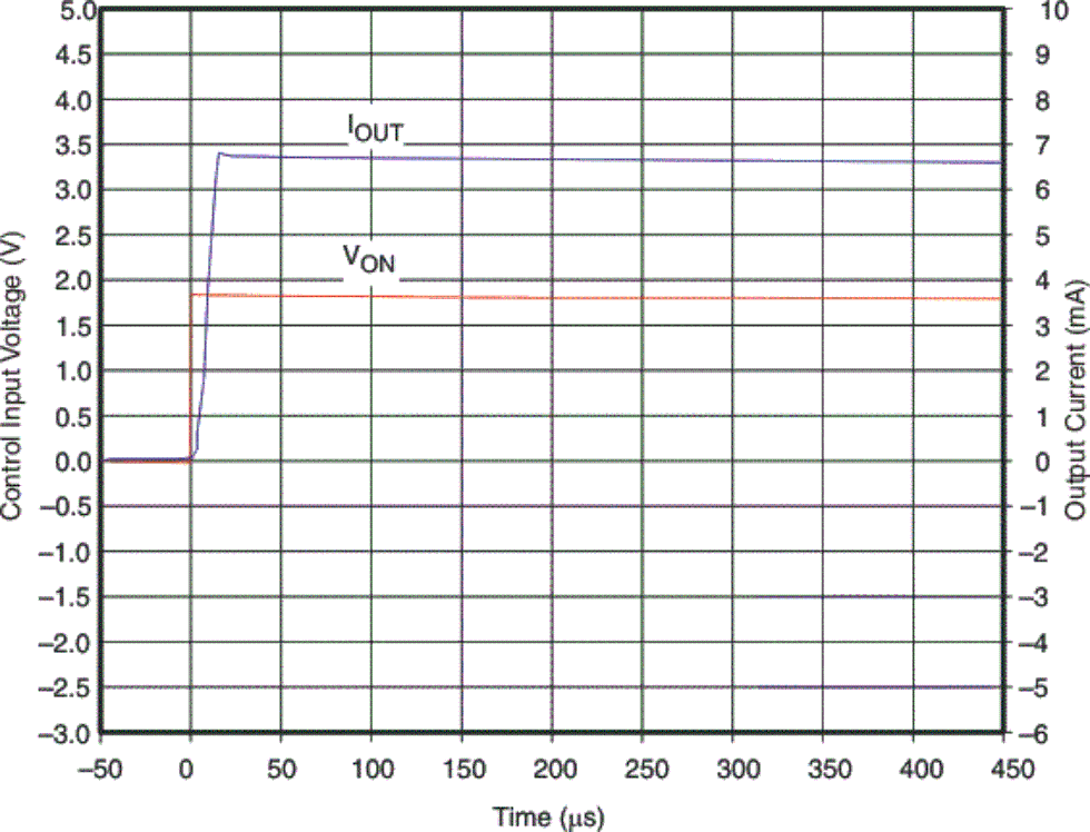
The undervoltage lockout turns off the switch if the input voltage drops below the undervoltage lockout threshold. With the ON pin active, the input voltage rising above the undervoltage lockout threshold causes a controlled turn-on of the switch, which limits current overshoots.
9.1.3 Reverse Voltage
If the voltage at the VOUT pin is larger than the VIN pin, large currents may flow and can cause permanent damage to the device. TPS22941/2/3/4/5 is designed to control current flow only from VIN to VOUT.
9.1.4 Input Capacitor
To limit the voltage drop on the input supply caused by transient in-rush currents when the switch turns on into a discharged load capacitor or a short-circuit, a capacitor needs to be placed between VIN and GND. A 1-μF ceramic capacitor, CIN, placed close to the pins is usually sufficient. Higher values of CIN can be used to further reduce the voltage drop.
9.1.5 Output Capacitor
A 0.1-μF capacitor, COUT, should be placed between VOUT and GND. This capacitor will prevent parasitic board inductances from forcing VOUT below GND when the switch turns off. For the TPS22941/2/3/4/5, the total output capacitance needs to be kept below a maximum value, COUT(MAX), to prevent the part from registering an over-current condition and turning-off the switch.
Due to the integrated body diode in the PMOS switch, a CIN greater than COUT is highly recommended. A COUT greater than CIN can cause VOUT to exceed VIN when the system supply is removed. This could result in current flow through the body diode from VOUT to VIN.
9.2 Typical Application
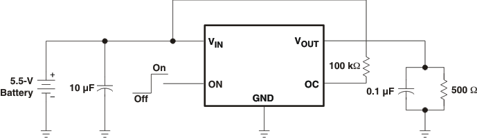 Figure 19. Typical Application Circuit, Active-High Enabled Device
 (TPS22943, TPS22944 and TPS22945 Only)
9.2.1 Design Requirements
For this design example, use the following as the input parameters:
| DESIGN PARAMETER | EXAMPLE VALUE |
|---|---|
| VIN | 5.0 V |
| Load Current | 50mA |
9.2.2 Detailed Design Procedure
To begin the design process, the designer needs to know the following:
- VIN voltage
- Load current
9.2.2.1 VIN to VOUT Voltage Drop
The VIN to VOUT voltage drop in the device is determined by the RON of the device and the load current. The RON of the device depends upon the VIN condition of the device. Refer to the RON specification of the device in the Electrical Characteristics table of this datasheet.
Once the RON of the device is determined based upon the VIN conditions, use Equation 1 to calculate the VIN to VOUT voltage drop:
where
- ΔV = voltage drop from VIN to VOUT
- ILOAD = load current
- RON = ON-resistance of the device for a specific VIN
9.2.2.2 Maximum Output Capacitance
When designing this device, it is important to ensure the inrush current of the output capacitance does not cause the device to exceed the current limiting time beyond the blanking time. The maximum output capacitance can be determined from Equation 2 :
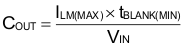
where
- COUT = output capacitance
- ILIM(MAX) = maximum current limit
- tBLANK(MIN) = minimum blanking time
- VIN = input voltage
9.2.2.3 Power Dissipation
During normal operation as a switch, the power dissipation is small and has little effect on the operating temperature of the part. The parts with the higher current limits will dissipate the most power and that will only be,
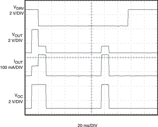
If the part goes into current limit the maximum power dissipation will occur when the output is shorted to ground. For TPS22941/2/5, the power dissipation scales by the auto-restart time (tRESTART) and the overcurrent blanking time (tBLANK) so that the maximum power dissipated is:
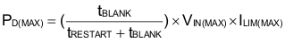
When using the TPS22943 and TPS22944, a short on the output causes the part to operate in a constant current state, dissipating a worst-case power as calculated above until the thermal shutdown activates. It then cycles in and out of thermal shutdown so long as the ON pin is active and the short is present.
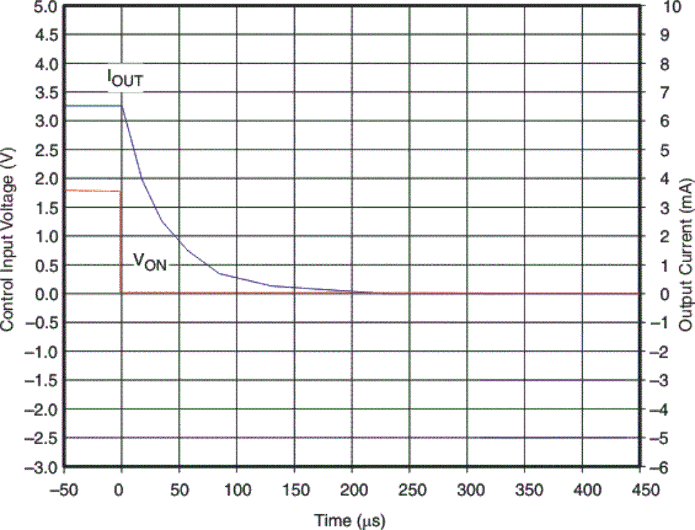
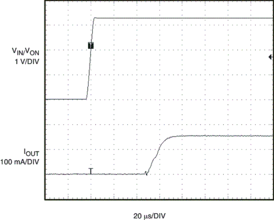
9.2.2.4 Application Curves
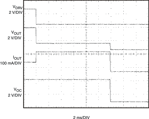
| VDRV signal forces the device to go into over-current mode. |
| CL = 0.1 µF | RL = 500 Ω | VIN = 3.3 V |
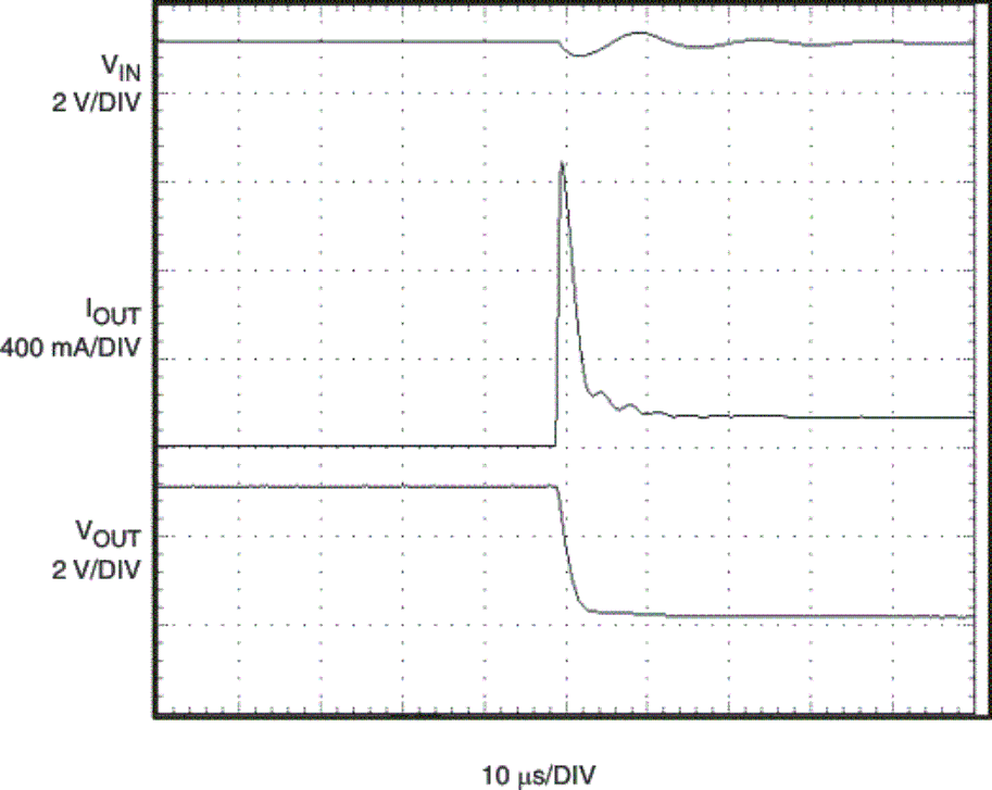
| CIN = 10 µF | COUT = 1 µF |
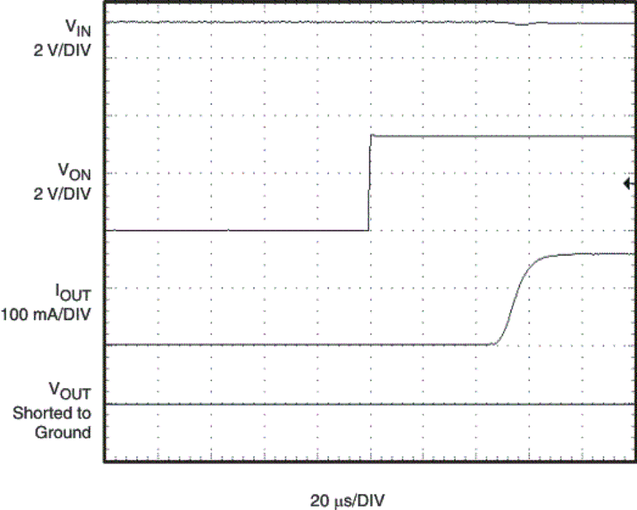
| CIN = 10 µF | COUT = 1 µF |
| VDRV signal forces the device to go into over-current mode. |
| CL = 0.1 µF | RL = 500 Ω | VIN = 3.3 V |
| CIN = 10 µF | COUT = 1 µF |