SLVS832D November 2008 – July 2014 TPS22941 , TPS22942 , TPS22943 , TPS22944 , TPS22945
PRODUCTION DATA.
- 1 Features
- 2 Applications
- 3 Description
- 4 Revision History
- 5 Device Comparison Table
- 6 Pin Configuration and Functions
- 7 Specifications
- 8 Detailed Description
- 9 Application and Implementation
- 10Power Supply Recommendations
- 11Layout
- 12Device and Documentation Support
- 13Mechanical, Packaging, and Orderable Information
Package Options
Mechanical Data (Package|Pins)
- DCK|5
Thermal pad, mechanical data (Package|Pins)
Orderable Information
6 Pin Configuration and Functions
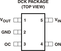
Pin Functions
| PIN | TYPE | DESCRIPTION | |
|---|---|---|---|
| NAME | SOT (DCK) PIN NO. |
||
| VOUT | 1 | O | Switch Output. Place ceramic bypass capacitor(s) between this terminal and GND. See the Application Information section for more information. |
| GND | 2 | – | Ground |
| OC | 3 | O | Over current output flag: active LOW, open drain output that indicates an over current, supply under voltage, or over temperature state. |
| ON | 4 | I | Switch control input. Do not leave floating. |
| VIN | 5 | I | Switch Input. Place ceramic bypass capacitor(s) between this terminal and GND. See the Application Information section for more information. |