SLVS914E April 2009 – April 2024 TPS22960
PRODUCTION DATA
- 1
- 1 Features
- 2 Applications
- 3 Description
- 4 Pin Configuration and Functions
- 5 Specifications
- 6 Parameter Measurement Information
- 7 Detailed Description
- 8 Application and Implementation
- 9 Device and Documentation Support
- 10Revision History
- 11Mechanical, Packaging, and Orderable Information
Package Options
Mechanical Data (Package|Pins)
Thermal pad, mechanical data (Package|Pins)
- DCN|8
Orderable Information
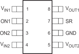
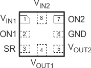
4 Pin Configuration and Functions
 Figure 4-1 DCN Package, 8-pin SOT (Top
View)
 Figure 4-2 RSE Package, 8-pin UQFN (Top
View)
Figure 4-2 RSE Package, 8-pin UQFN (Top
View)Table 4-1 Pin Functions
| PIN | I/O | DESCRIPTION | ||
|---|---|---|---|---|
| NAME | SOT | UQFN | ||
| VIN1 | 1 | 1 | I | Switch 1 input; bypass this input with a ceramic capacitor to GND. |
| ON1 | 2 | 2 | I | Switch 1 control input, active high. Do not leave floating. |
| ON2 | 3 | 7 | I | Switch 2 control input, active high. Do not leave floating. |
| VIN2 | 4 | 8 | I | Switch 2 input; bypass this input with a ceramic capacitor to GND. |
| VOUT2 | 5 | 5 | O | Switch 2 output. |
| GND | 6 | 6 | — | Ground. |
| SR | 7 | 3 | I | Slew rate control pin. SR = GND translates into a 75-μs rise time; SR = high translates into a 660-μs rise time. |
| VOUT1 | 8 | 4 | O | Switch 1 output. |