SLVSCP7B November 2014 – March 2016 TPS22968-Q1
PRODUCTION DATA.
- 1 Features
- 2 Applications
- 3 Description
- 4 Revision History
- 5 Device Comparison Table
- 6 Pin Configuration and Functions
-
7 Specifications
- 7.1 Absolute Maximum Ratings
- 7.2 ESD Ratings
- 7.3 Recommended Operating Conditions
- 7.4 Thermal Information
- 7.5 Electrical Characteristics (VBIAS = 5 V)
- 7.6 Electrical Characteristics (VBIAS = 3.3 V)
- 7.7 Electrical Characteristics (VBIAS = 2.5 V)
- 7.8 Switching Characteristics
- 7.9 Typical Characteristics
- 8 Parameter Measurement Information
- 9 Detailed Description
- 10Application and Implementation
- 11Power Supply Recommendations
- 12Layout
- 13Device and Documentation Support
- 14Mechanical, Packaging, and Orderable Information
Package Options
Mechanical Data (Package|Pins)
- DMG|10
Thermal pad, mechanical data (Package|Pins)
- DMG|10
Orderable Information
1 Features
- Integrated Dual Channel Load Switch
- Qualified for Automotive Applications:
- Device Temperature Grade 1 : –40°C to +125°C Ambient Operating Temperature Range
- Input Voltage Range: 0.8 to 5.5 V
- VBIAS Voltage Range: 2.5 to 5.5 V
- On-Resistance
- RON = 29 mΩ at VIN = 5 V (VBIAS = 5 V)
- RON = 27 mΩ at VIN = 3.3 V (VBIAS = 5 V)
- RON = 26 mΩ at VIN = 1.8 V (VBIAS = 5 V)
- 4-A Maximum Continuous Switch Current per Channel
- Low Quiescent Current
- 58-µA at VBIAS = 5 V (Both Channels)
- Low-Control Input-Threshold Enables Use of 1.2-, 1.8-, 2.5-, 3.3- V Logic
- Configurable Rise Time With CT Pin(1)
- Quick-Output Discharge (QOD)(2) (TPS22968-Q1 Only)
- 10-Pin WSON Package With Wettable Flanks
- ESD Performance Tested per JEDEC STD
- ±2-kV HBM and ±1-kV CDM
- Latch-Up Performance meets 100-mA per JESD 78, Class II
- GPIO Enable – Active High (1) (2)
2 Applications
- Automotive Electronics
- Infotainment
- Cluster
- ADAS
3 Description
The TPS22968x-Q1 is a small, dual-channel load switch with configurable rise time. The device contains two N-channel MOSFETs that can operate over an input voltage range of 0.8 V to 5.5 V and can support a maximum continuous current of 4-A per channel. Each switch is independently controlled by an on/off input (ON1 and ON2), which is capable of interfacing directly with low-voltage control signals. The TPS22968-Q1 includes a 270 Ω on-chip resistor for quick output discharge when the switch is turned off.
The TPS22968x-Q1 is available in a small, space-saving package (DMG) with wettable flanks and an integrated thermal pad. The wettable flanks allow for visual solder inspection. The device is characterized for operation over the free-air temperature range of –40 to +125°C.
Device Information (1)
| PART NUMBER | PACKAGE | BODY SIZE (NOM) |
|---|---|---|
| TPS22968-Q1 TPS22968N-Q1 |
WSON (10) | 2.00 mm × 3.00 mm |
- For all available packages, see the orderable addendum at the end of the data sheet.
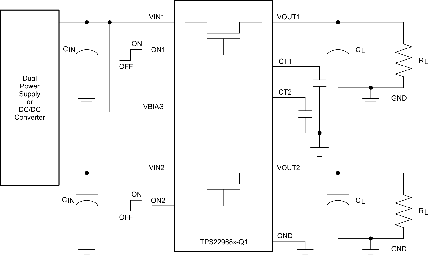
Typical Application Schematic
