SLVSCP7B November 2014 – March 2016 TPS22968-Q1
PRODUCTION DATA.
- 1 Features
- 2 Applications
- 3 Description
- 4 Revision History
- 5 Device Comparison Table
- 6 Pin Configuration and Functions
-
7 Specifications
- 7.1 Absolute Maximum Ratings
- 7.2 ESD Ratings
- 7.3 Recommended Operating Conditions
- 7.4 Thermal Information
- 7.5 Electrical Characteristics (VBIAS = 5 V)
- 7.6 Electrical Characteristics (VBIAS = 3.3 V)
- 7.7 Electrical Characteristics (VBIAS = 2.5 V)
- 7.8 Switching Characteristics
- 7.9 Typical Characteristics
- 8 Parameter Measurement Information
- 9 Detailed Description
- 10Application and Implementation
- 11Power Supply Recommendations
- 12Layout
- 13Device and Documentation Support
- 14Mechanical, Packaging, and Orderable Information
Package Options
Mechanical Data (Package|Pins)
- DMG|10
Thermal pad, mechanical data (Package|Pins)
- DMG|10
Orderable Information
6 Pin Configuration and Functions
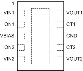
DMG Package
|
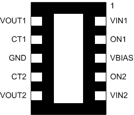
DMG Package
|
Pin Functions
| PIN | I/O | DESCRIPTION | |
|---|---|---|---|
| NO. | NAME | ||
| 1 | VIN1 | I | Switch 1 input. Bypass this input with a ceramic capacitor to GND. |
| 2 | ON1 | I | Active-high switch 1 control input. Do not leave floating. |
| 3 | VBIAS | I | Bias voltage. Power supply to the device. Recommended voltage range for this pin is 2.5 to 5.5 V. See VIN and VBIAS Voltage Range section. |
| 4 | ON2 | I | Active-high switch 2 control input. Do not leave floating. |
| 5 | VIN2 | I | Switch 2 input. Bypass this input with a ceramic capacitor to GND. |
| 6 | VOUT2 | O | Switch 2 output |
| 7 | CT2 | O | Switch 2 slew rate control. Can be left floating. |
| 8 | GND | — | Ground |
| 9 | CT1 | O | Switch 1 slew rate control. Can be left floating. |
| 10 | VOUT1 | O | Switch 1 output |
| — | Thermal Pad | — | Thermal pad (exposed center pad) to alleviate thermal stress. Tie to GND. See Layout Guidelines section. |

