SLVSFT0A July 2021 – December 2021 TPS22992
PRODUCTION DATA
- 1 Features
- 2 Applications
- 3 Description
- 4 Revision History
- 5 Device Comparison Table
- 6 Pin Configuration and Functions
-
7 Specifications
- 7.1 Absolute Maximum Ratings
- 7.2 ESD Ratings
- 7.3 Recommended Operating Conditions
- 7.4 Thermal Information
- 7.5 Electrical Characteristics (VBIAS = 5 V)
- 7.6 Electrical Characteristics (VBIAS = 3.3 V)
- 7.7 Electrical Characteristics (VBIAS = 1.5 V)
- 7.8 Switching Characteristics (VBIAS = 5 V)
- 7.9 Switching Characteristics (VBIAS = 3.3 V)
- 7.10 Switching Characteristics (VBIAS = 1.5 V)
- 7.11 Typical Characteristics
- 8 Timing Diagram
- 9 Detailed Description
- 10Application and Implementation
- 11Power Supply Recommendations
- 12Layout
- 13Device and Documentation Support
- 14Mechanical, Packaging, and Orderable Information
Package Options
Mechanical Data (Package|Pins)
Thermal pad, mechanical data (Package|Pins)
Orderable Information
3 Description
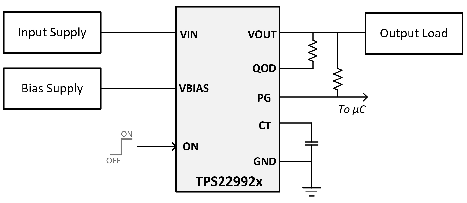
The TPS22992x product family consists of two devices: TPS22992 and TPS22992S. Each device is a single-channel load switch with an 8.7-mΩ power MOSFET designed to maximize power density in applications up to 5.5 V and 6 A. A configurable rise time provides flexibility for power sequencing and minimizes inrush current for high capacitance loads.
The switch is controlled by an enable pin (ON), which is capable of interfacing directly with low voltage GPIO signals (VIH = 0.8 V). The TPS22992x device has an optional QOD pin for quick output discharge when switch is turned off, and the fall time (tFALL) of the output can be adjusted through an external resistor. There is a Power Good (PG) signal on the device that indicates when the main MOSFET is fully turned on, which can be used to enable a downstream load.
Both TPS22992x devices come with thermal shutdown to ensure protection in high temperature environments. The TPS22992S device also integrates overcurrent protection, preventing damage to the device if the output is shorted to ground during operation or start-up.
For small form factor applications, the TPS22992x devices are available in a 1.25 × 1.25mm, 0.4-mm pitch, 8-pin WQFN package. The TPS22992 device is also available in a 1.5 × 1.25 mm, 0.5-mm pitch, 8-pin WQFN package where a wider pin pitch is needed. Both devices are characterized for operation over the free-air temperature range of –40°C to +125°C.
| PART NUMBER | PACKAGE(1) | BODY SIZE (NOM) |
|---|---|---|
TPS22992 | WQFN - 8 (RXP) | 1.5 mm × 1.25 mm |
TPS22992S | WQFN - 8 (RXN) | 1.25 mm × 1.25 mm |
 TPS2299x Application for Power Sequencing