SLVSF02E march 2019 – may 2023 TPS23881
PRODUCTION DATA
- 1
- 1 Features
- 2 Applications
- 3 Description
- 4 Revision History
- 5 Device Comparison Table
- 6 Pin Configuration and Functions
- 7 Specifications
- 8 Parameter Measurement Information
-
9 Detailed Description
- 9.1 Overview
- 9.2 Functional Block Diagram
- 9.3 Feature Description
- 9.4 Device Functional Modes
- 9.5 I2C Programming
- 9.6
Register Maps
- 9.6.1 Complete Register Set
- 9.6.2
Detailed Register Descriptions
- 9.6.2.1 INTERRUPT Register
- 9.6.2.2 INTERRUPT MASK Register
- 9.6.2.3 POWER EVENT Register
- 9.6.2.4 DETECTION EVENT Register
- 9.6.2.5 FAULT EVENT Register
- 9.6.2.6 START/ILIM EVENT Register
- 9.6.2.7 SUPPLY and FAULT EVENT Register
- 9.6.2.8 CHANNEL 1 DISCOVERY Register
- 9.6.2.9 CHANNEL 2 DISCOVERY Register
- 9.6.2.10 CHANNEL 3 DISCOVERY Register
- 9.6.2.11 CHANNEL 4 DISCOVERY Register
- 9.6.2.12 POWER STATUS Register
- 9.6.2.13 PIN STATUS Register
- 9.6.2.14 OPERATING MODE Register
- 9.6.2.15 DISCONNECT ENABLE Register
- 9.6.2.16 DETECT/CLASS ENABLE Register
- 9.6.2.17 Power Priority / 2Pair PCUT Disable Register Name
- 9.6.2.18 TIMING CONFIGURATION Register
- 9.6.2.19 GENERAL MASK Register
- 9.6.2.20 DETECT/CLASS RESTART Register
- 9.6.2.21 POWER ENABLE Register
- 9.6.2.22 RESET Register
- 9.6.2.23 ID Register
- 9.6.2.24 Connection Check and Auto Class Status Register
- 9.6.2.25 2-Pair Police Ch-1 Configuration Register
- 9.6.2.26 2-Pair Police Ch-2 Configuration Register
- 9.6.2.27 2-Pair Police Ch-3 Configuration Register
- 9.6.2.28 2-Pair Police Ch-4 Configuration Register
- 9.6.2.29 Capacitance (Legacy PD) Detection
- 9.6.2.30 Power-on Fault Register
- 9.6.2.31 PORT RE-MAPPING Register
- 9.6.2.32 Channels 1 and 2 Multi Bit Priority Register
- 9.6.2.33 Channels 3 and 4 Multi Bit Priority Register
- 9.6.2.34 4-Pair Wired and Port Power Allocation Register
- 9.6.2.35 4-Pair Police Ch-1 and 2 Configuration Register
- 9.6.2.36 4-Pair Police Ch-3 and 4 Configuration Register
- 9.6.2.37 TEMPERATURE Register
- 9.6.2.38 4-Pair Fault Configuration Register
- 9.6.2.39 INPUT VOLTAGE Register
- 9.6.2.40 CHANNEL 1 CURRENT Register
- 9.6.2.41 CHANNEL 2 CURRENT Register
- 9.6.2.42 CHANNEL 3 CURRENT Register
- 9.6.2.43 CHANNEL 4 CURRENT Register
- 9.6.2.44 CHANNEL 1 VOLTAGE Register
- 9.6.2.45 CHANNEL 2 VOLTAGE Register
- 9.6.2.46 CHANNEL 3 VOLTAGE Register
- 9.6.2.47 CHANNEL 4 VOLTAGE Register
- 9.6.2.48 2x FOLDBACK SELECTION Register
- 9.6.2.49 FIRMWARE REVISION Register
- 9.6.2.50 I2C WATCHDOG Register
- 9.6.2.51 DEVICE ID Register
- 9.6.2.52 CHANNEL 1 DETECT RESISTANCE Register
- 9.6.2.53 CHANNEL 2 DETECT RESISTANCE Register
- 9.6.2.54 CHANNEL 3 DETECT RESISTANCE Register
- 9.6.2.55 CHANNEL 4 DETECT RESISTANCE Register
- 9.6.2.56 CHANNEL 1 DETECT CAPACITANCE Register
- 9.6.2.57 CHANNEL 2 DETECT CAPACITANCE Register
- 9.6.2.58 CHANNEL 3 DETECT CAPACITANCE Register
- 9.6.2.59 CHANNEL 4 DETECT CAPACITANCE Register
- 9.6.2.60 CHANNEL 1 ASSIGNED CLASS Register
- 9.6.2.61 CHANNEL 2 ASSIGNED CLASS Register
- 9.6.2.62 CHANNEL 3 ASSIGNED CLASS Register
- 9.6.2.63 CHANNEL 4 ASSIGNED CLASS Register
- 9.6.2.64 AUTO CLASS CONTROL Register
- 9.6.2.65 CHANNEL 1 AUTO CLASS POWER Register
- 9.6.2.66 CHANNEL 2 AUTO CLASS POWER Register
- 9.6.2.67 CHANNEL 3 AUTO CLASS POWER Register
- 9.6.2.68 CHANNEL 4 AUTO CLASS POWER Register
- 9.6.2.69 ALTERNATIVE FOLDBACK Register
- 9.6.2.70 SRAM CONTROL Register
- 10Application and Implementation
- 11Power Supply Recommendations
- 12Layout
- 13Device and Documentation Support
- 14Mechanical, Packaging, and Orderable Information
Package Options
Mechanical Data (Package|Pins)
- RTQ|56
Thermal pad, mechanical data (Package|Pins)
- RTQ|56
Orderable Information
9.6.2.48 2x FOLDBACK SELECTION Register
COMMAND = 40h with1 Data Byte Read/Write
| 7 | 6 | 5 | 4 | 3 | 2 | 1 | 0 |
| 2xFB4 | 2xFB3 | 2xFB2 | 2xFB1 | MPOL4 | MPOL3 | MPOL2 | MPOL1 |
| R/W-0 | R/W-0 | R/W-0 | R/W-0 | R/W -0 | R/W -0 | R/W -0 | R/W -0 |
| LEGEND: R/W = Read/Write; R = Read only; -n = value after reset |
| Bit | Field | Type | Reset | Description | ||||
|---|---|---|---|---|---|---|---|---|
| 7–4 | 2xFB4- 2xFB1 | R/W | 0 | When set, this activates the 2x Foldback mode for a channel which increases its ILIM and ISHORT levels normal settings, as shown in Figure 9-3. Note that the fault timer starts when the ILIM threshold is exceeded. | ||||
| Notes: | ||||||||
| 1) | At turn on, the inrush current profile is unaffected by these bits, as shown in Figure 9-2. | |||||||
| 2) | When a 2xFBn bit is deasserted, the tLIM setting used for the associated channel is always the nominal value (approximately 60 ms). If 2xFBn bit is asserted, then tLIM for associated channel is programmable as defined in the Timing Configuration register (0x16). | |||||||
| 3) | If the assigned class for a channel is class 4 or above, the 2xFB bit will be automatically set during turn on.
For a single signature 4-pair powered PD both bits will be set For a dual signature 4-pair powered PD each Channel will be set according to the individually assigned PD classification | |||||||
| 3-0 | MPOL4 - MPOL1 | R/W | 0 | Manual Policing and Foldback configuration bits
0 = The internal device firmware automatically adjusts the Policing (PCUT) and 2xFBn settings based on the assigned class during port turn on 1 = The Policing (PCUT) and 2xFBn settings will not be changed during port turn on. Note: Independent of these settings, the Policing (PCUT) and 2xFBn settings are returned to their default values upon port turn off. Note: Setting either bit for a 4P configured port disables the automatic configuration on both channels The MPOLn bits are cleared upon port turn off. | ||||
For 4-pair wired Ports the 2xFBn bits individually control each Channels operation.
Refer to register 0x55h description for more information on additional Foldback and Inrush configuration options
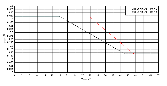
 Figure 9-56 1x
Mode (2xFBn = 0) Foldback Curves, IPORT vs
VDRAIN
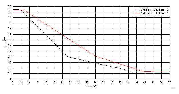
 Figure 9-57 2x
Mode (2xFBn = 1) Foldback Curves, IPORT vs
VDRAIN