SLVSCV6A January 2015 – February 2015 TPS24740 , TPS24741 , TPS24742
PRODUCTION DATA.
- 1 Features
- 2 Applications
- 3 Description
- 4 Simplified Schematics
- 5 Revision History
- 6 Device Comparison Table
- 7 Pin Configuration and Functions
- 8 Specifications
-
9 Detailed Description
- 9.1 Overview
- 9.2 Functional Block Diagram
- 9.3
Feature Description
- 9.3.1 Internal Power ORing of TPS24740
- 9.3.2 Enable and Over-voltage Protection
- 9.3.3 Current Limit and Power Limit During Start-up
- 9.3.4 Two Level Protection During Regular Operation
- 9.3.5 Dual Timer (TFLT and TINR)
- 9.3.6 Using SoftStart - IHGATE and TINR Considerations
- 9.3.7 Three Options for Response to a Fast Trip
- 9.3.8 Programmable Reverse Voltage Threshold
- 9.3.9 Analog Current Monitor
- 9.3.10 Power Good Flag
- 9.3.11 ORing MOSFET Status Indicator
- 9.3.12 Fault Reporting
- 9.4 Device Functional Modes
-
10Application and Implementation
- 10.1 Application Information
- 10.2
Typical Application
- 10.2.1 30A Single channel OR then Hot Swap With Current Monitoring
- 10.2.2 Design Requirements
- 10.2.3
Detailed Design Procedure
- 10.2.3.1 Select RSNS and VSNS,CL Setting
- 10.2.3.2 Selecting the Fast Trip Threshold and Filtering
- 10.2.3.3 Selecting the Hot Swap FET(s)
- 10.2.3.4 Select Power Limit
- 10.2.3.5 Set Fault Timer
- 10.2.3.6 Check MOSFET SOA
- 10.2.3.7 Choose ORing MOSFET
- 10.2.3.8 Choose Reverse Current Threshold and Filtering
- 10.2.3.9 Choose Under Voltage and Over Voltage Settings
- 10.2.3.10 Selecting CIN, COUT, and CMIDDLE
- 10.2.3.11 Selecting D1 and D2
- 10.2.3.12 Ensuring Stability
- 10.2.3.13 Compute Tolerances
- 10.2.4 Application Curves
- 10.2.5
40 A Single Channel Hot Swap then ORing
- 10.2.5.1 Design Requirements
- 10.2.5.2
Design Procedure
- 10.2.5.2.1 Select RSNS and VSNS,CL Setting
- 10.2.5.2.2 Selecting the Fast Trip Threshold and Filtering
- 10.2.5.2.3 Selecting the Hot Swap FET
- 10.2.5.2.4 Select Power Limit
- 10.2.5.2.5 Set Fault Timer
- 10.2.5.2.6 Check MOSFET SOA
- 10.2.5.2.7 Checking Stability of Hot Swap Loop
- 10.2.5.2.8 Choose ORing MOSFET
- 10.2.5.2.9 Choose Reverse Current Threshold and Filtering
- 10.2.5.2.10 Choose Under Voltage and Over Voltage Settings
- 10.2.5.2.11 Selecting CIN, COUT, CMIDDLE, and Transient Protection
- 10.2.5.2.12 Adding CENHS
- 10.2.5.3 Application Curves
- 10.3 System Examples
- 11Power Supply Recommendations
- 12Layout
- 13Device and Documentation Support
- 14Mechanical, Packaging, and Orderable Information
Package Options
Mechanical Data (Package|Pins)
- RGE|24
Thermal pad, mechanical data (Package|Pins)
- RGE|24
Orderable Information
8 Specifications
8.1 Absolute Maximum Ratings
Unless otherwise noted, these apply over recommended operating junction temperature: -40°C ≤ TJ ≤ 125°C. (1)(1) Stresses beyond those listed under Absolute Maximum Ratings may cause permanent damage to the device. These are stress ratings only, which do not imply functional operation of the device at these or any other conditions beyond those indicated under Recommended Operating Conditions. Exposure to absolute-maximum-rated conditions for extended periods may affect device reliability.
8.2 ESD Ratings
| VALUE | UNIT | |||
|---|---|---|---|---|
| V(ESD)(1) | Electrostatic discharge | Human-body model (HBM), per ANSI/ESDA/JEDEC JS-001(2) | ±1500 | V |
| Charged-device model (CDM), per JEDEC specification JESD22-C101(3) | ±500 | |||
(1) Electrostatic discharge (ESD) measures device sensitivity and immunity to damage caused by assembly line electrostatic discharges into the device.
(2) JEDEC document JEP155 states that 500-V HBM allows safe manufacturing with a standard ESD control process.
(3) JEDEC document JEP157 states that 250-V CDM allows safe manufacturing with a standard ESD control process.
8.3 Recommended Operating Conditions
These apply over recommended operating junction temperature: -40°C ≤ TJ ≤ 125°C.| MIN | MAX | UNIT | ||
|---|---|---|---|---|
| Input voltage | VDD, SENM, SET(1), FSTP | 2.5 | 18 | V |
| ENHS, ENOR, FLTb, PGHS, STAT, OUTH | 0 | 18 | ||
| A, C, RVSNM, RVSNP; (2) | 0.7 | 18 | ||
| Sink current | FLTb, PGHS, STAT | 0 | 2 | mA |
| Source current | IMON | 0 | 1 | mA |
| External resistance | PLIM | 4.99 | 500 | kΩ |
| IMON | 1 | 6 | kΩ | |
| RVSNP | 10 | 1000 | Ω | |
| FSTP | 10 | 4000 | Ω | |
| SET | 10 | 400 | Ω | |
| RIMON / RSET | w/o RSTBL(4) | 10 | 70 | |
| With appropriate RSTBL | 3 | 10 | ||
| External capacitor | CP, FSTP, RVSNP | 1 | 1000 | nF |
| HGATE, BGATE (3) | 0 | 1 | µF | |
| TINR, TFLT | 1 | nF | ||
| IMON | 30 | pF | ||
| IMONBUF | 100 | pF | ||
| Operating junction temperature, TJ | –40 | 125 | °C | |
(1) Do not apply voltage to these pins.
(2) For the HS then ORing application these pins may be below the recommended minimum during start-up. The part is designed to function properly under these scenarios. However the part should not be used with a bus voltage below the recommended voltage.
(3) External capacitance tied to HGATE, BGATE should be in series with a resistor no less than 1kΩ.
(4) Refer to RSTBL Requirement for RIMON / RSET < 10 describe in section Select RSNS and VSNS,CL Setting.
8.4 Thermal Information
| THERMAL METRIC(1) | TPS24740, TPS24741, TPS24742 | UNIT | |
|---|---|---|---|
| RGE (24 PINS) | |||
| RθJA | Junction-to-ambient thermal resistance | 34.6 | °C/W |
| RθJC(top) | Junction-to-case (top) thermal resistance | 38.4 | |
| RθJB | Junction-to-board thermal resistance | 12.9 | |
| ψJT | Junction-to-top characterization parameter | 0.5 | |
| ψJB | Junction-to-board characterization parameter | 12.9 | |
| RθJC(bot) | Junction-to-case (bottom) thermal resistance | 3.2 | |
(1) For more information about traditional and new thermal metrics, see the IC Package Thermal Metrics application report, SPRA953.
8.5 Electrical Characteristics
Unless otherwise noted these limits apply to the following: -40°C ≤ TJ ≤ 125°C; 2.5V < VVDD , VOUTH < 18V; 0.7 V < VA , VC , VRVSNM < 18 V; VENHS = VENOR = 2 V, VOV = 0 V; VBGATE, VHGATE, VPGHS, VSTAT, VFLTb, and VIMONBUF are floating; CCP = 100 nF, CINR = 1 nF, CFLT = 1 nF, RSET = 44.2 Ω, RIMON = 2.98 kΩ, RFSTP = 200 Ω, RRV = 200 Ω, and RPLIM = 52 kΩ.| PARAMETER | TEST CONDITION | MIN | TYP | MAX | UNIT | |
|---|---|---|---|---|---|---|
| INPUT SUPPLY (VDD) | ||||||
| VUVR | UVLO threshold, rising | 2.2 | 2.32 | 2.45 | V | |
| VUVhyst | UVLO hysteresis | 0.1 | V | |||
| IQON | Supply current: IVDD+IA+IC+ IOUTH | Device on, VENHS = VENOR = 2V | 4.2 | 6 | mA | |
| HOT SWAP FET ENABLE (ENHS) | ||||||
| VENHS | Threshold voltage, rising | 1.3 | 1.35 | 1.4 | V | |
| VENHShyst | Hysteresis | 50 | mV | |||
| IENHS | Input Leakage Current | 0 ≤ VENHS ≤ 30V | –1 | 1 | µA | |
| BLOCKING (ORING) FET ENABLE (ENOR) | ||||||
| VENOR | Threshold voltage, rising | 1.3 | 1.35 | 1.4 | V | |
| VENORhyst | Hysteresis | 50 | mV | |||
| IENOR | Input leakage current | 0 V ≤ VENOR ≤ 30V | –1 | 0 | 1 | µA |
| OVER VOLTAGE (OV) | ||||||
| VOVR | Threshold voltage, rising | 1.3 | 1.35 | 1.4 | mV | |
| VOVhyst | Hysteresis | 50 | mV | |||
| IOV | Input leakage current | 0 ≤ VOV ≤ 30V | –1 | 1 | µA | |
| POWER LIMIT PROGRAMING (PLIM) | ||||||
| VPLIM,BIAS | Bias voltage | Sourcing 10μA | 0.66 | 0.675 | 0.69 | V |
| VIMON,PL | Regulated IMON voltage during power limit | RPLIM = 52 kΩ; VSENM-OUTH=12V; | 114.75 | 135 | 155.25 | mV |
| RPLIM = 105 kΩ; VSENM-OUTH=12V; | 56.95 | 67 | 77.05 | |||
| RPLIM = 261 kΩ; VSENM-OUTH=12V; | 18.9 | 27 | 35.1 | |||
| RPLIM = 105 kΩ; VSENM-OUTH=2V; | 341.7 | 402 | 462.3 | |||
| RPLIM = 105 kΩ; VSENM-OUTH=18V; | 38.25 | 45 | 51.75 | |||
| SLOW TRIP THRESHOLD (SET) | ||||||
| VOS_SET | Input referred offset (VSNS to VIMON scaling) | RSET = 44.2Ω; RIMON=3kΩ to 1.2kΩ (corresponds to VSNS,CL=10mV to 25mV) | –150 | 150 | µV | |
| VGE_SET | Gain error (VSNS to VIMON scaling)(1) | –0.4% | 0.4% | |||
| FAST TRIP THRESHOLD PROGRAMMING (FSTP) | ||||||
| IFSTP | FSTP input bias current | VFSTP=12V | 95 | 100 | 105 | µA |
| VFASTRIP | Fast trip threshold | RFSTP = 200 Ω, VSNS when VHGATE ↓ | 18 | 20 | 22 | mV |
| RFSTP = 1 kΩ, VSNS when VHGATE ↓ | 95 | 100 | 105 | |||
| RFSTP = 4 kΩ, VSNS when VHGATE ↓ | 380 | 400 | 420 | |||
| CURRENT MONITOR and CURRENT LIMIT PROGRAMING (IMON) | ||||||
| VIMON,CL | Slow trip threshold at summing node | VIMON↑, when ITFLT starts sourcing | 660 | 675 | 690 | mV |
| CURRENT MONITOR (IMONBUF) | ||||||
| VOS_IMONBUF | Buffer offset | VIMON = 50mV to 675mV, Input referred | –3 | 0 | 3 | mV |
| GAINIMONBUF | Buffer voltage gain | ΔVIMONBUFF / ΔVIMON | 2.97 | 2.99 | 3.01 | V |
| BWIMONBUF | Buffer closed loop bandwidth | CIMONBUF = 75pF | 1 | MHz | ||
| HOT SWAP GATE DRIVER (HGATE) | ||||||
| VHGATE | HGATE output voltage | 5 ≤ VVDD ≤ 16V; measure VHGATE-OUTH | 12 | 13.6 | 15.5 | V |
| 2.5V <VVDD < 5V; 16V <VVDD < 20V measure VHGATE-OUTH |
7 | 7.95 | 15 | V | ||
| VHGATEmax | Clamp voltage | Inject 10μA into HGATE, measure V(HGATE – OUTH) | 12 | 13.9 | 15.5 | V |
| IHGATEsrc | Sourcing current | VHGAT-OUTH = 2V-10V | 44 | 55 | 66 | µA |
| IHGATEfastSink | Sinking current for fast trip | VHGATE-OUTH = 2V -15V; V(FSTP – SENM) = 20mV | 0.45 | 1 | 1.6 | A |
| IHGATEsustSink | Sustained sinking current | Sustained, VHGATE-OUTH = 2V – 15V; VENHS = 0 | 30 | 44 | 60 | mA |
| CURRENT SENSE NEGATIVE INPUT (SENM) | ||||||
| ISENM | Input bias current | VSENM = 12V | 15 | 20 | µA | |
| INRUSH TIMER (TINR) | ||||||
| ITINRsrc | Sourcing current | VTINR = 0V, In power limit or current limit | 8 | 10.25 | 12.5 | µA |
| ITINRsink | Sinking current | VTINR = 2V, In regular operation | 1.5 | 2 | 2.5 | µA |
| VTINRup | Upper threshold voltage | Raise VTINR until HGATE starts sinking | 1.3 | 1.35 | 1.4 | V |
| VTINRlr | Lower threshold voltage | Raise VTINR to 2V. Reduce VTINR until ITINR is sourcing. | 0.33 | 0.35 | 0.37 | v |
| RTINR | Bleed down resistance | VVDD = 0V, VTINR = 2V | 70 | 104 | 130 | kΩ |
| ITINR-PD | Pulldown current | VTINR = 2V, when VENHS = 0V | 2 | 4.2 | 7 | mA |
| VIMON,TINR | See (2) | RPLIM = 52kΩ, VSENM = 12V, VOUTH = 0 V. Raise IMON voltage and record IMON when TINR starts sourcing current | 47.75 | 90 | 132.25 | mV |
| VIMON,PL | See (2) | RPLIM = 52kΩ, VSENM = 12V, VOUTH = 0 V. Raise IMON voltage and record IMON when IHGATE starts sinking current. | 114.75 | 135 | 155.25 | mV |
| ΔVIMON,TINR | See (2) | RPLIM = 52kΩ, VSENM = 12V, VOUTH = 0 V. ΔVIMON,TINR = VIMON,PL – VIMON,TINR |
23 | 45 | 67 | mV |
| FAULT TIMER (TFLT) | ||||||
| ITFLTsrc | Sourcing current | VTFLT = 0V, PGHS is high and in overcurrent | 8 | 10.25 | 12.5 | µA |
| ITFLTsink | Sinking current | VTFLT = 2V, Not in overcurrent | 1.5 | 2 | 2.5 | µA |
| VTFLTup | Upper threshold voltage | Raise VTFLT until HGATE starts sinking | 1.3 | 1.35 | 1.4 | V |
| RTFLT | Bleed down resistance | VVDD = 0V, VTFLT = 2V | 70 | 104 | 130 | kΩ |
| ITFLT-PD | Pulldown current | VTFLT = 2V, when VENHS = 0V | 2 | 5.6 | 7 | mA |
| HOT SWAP OUTPUT (OUTH) | ||||||
| IOUTH, BIAS | Input bias current | VOUTH = 12V | 30 | 70 | µA | |
| CHARGE PUMP FOR BGATE (CP) | ||||||
| ICP | CP Equivalent charging resistance | VA = 12 V , 1mA CP current | 5 | 8.7 | 12.5 | kΩ |
| VCP | CP Output voltage | Max(VA, VC, VVDD) > 6 V, Measure VCP-A | 9 | 10 | 11 | V |
| 6V > Max(VA, VC, VVDD) > 4V, Measure VCP-A | 5 | 5.9 | 11 | |||
| Max(VA, VC, VVDD) = 2.5 V, Measure VCP-A | 8 | 9.8 | 11 | |||
| BLOCKING/ORING GATE DRIVER (BGATE) | ||||||
| IBGATE_CHRG | BGATE Pull up current | VAC = 20mV, pulse | 30 | mA | ||
| VAC = 20mV, sustained | 0.2 | 0.3 | 0.4 | mA | ||
| IBGATEsustSink | BGATE Sinking current | Fast turnoff, VBGATE-A = 7V | 0.4 | 0.9 | 1.4 | A |
| Sustained, VBGATE-A = 2V to 11V | 19 | 35 | 65 | mA | ||
| BLOCKING/ORing ANODE (A) | ||||||
| IA | Input current(3) | 2.5 V ≤ VA ≤ 18V | 3 | mA | ||
| VA_UVLO | Undervoltage lockout | VA increasing and VVDD=VC=0.7V | 1.85 | 1.93 | 2.05 | V |
| VA_UVLO_hyst | Undervoltage lockout hysteresis | 0.1 | V | |||
| BLOCKING/ORing CATHODE (C) | ||||||
| IC | Input current(3) | 2.5 V ≤ VC ≤ 18V | 3 | mA | ||
| VC_UVLO | Undervoltage lockout | VC increasing and VDD=VA=0.7V | 1.85 | 1.93 | 2.05 | V |
| VC_UVHyst | Hysteresis | 100 | mV | |||
| VFWDTH | Forward turn-on voltage | Measure VAC when VBGATE ↑ | 7.5 | 10 | 12.5 | mV |
| POSITIVE INPUT OF REVERSE VOLTAGE COMPARATOR (RVSNP) | ||||||
| IRVSNP | RVSNP Input bias current | VRVSNP = 12V, sinking current; 0.7V < VA, VRVSNM < 20V |
93 | 99 | 105 | µA |
| VRVTRIP1 | Reverse Comparator Offset | RRV=10Ω, Measure VRVSNP-RVSNM, when BGATE↓ | -1 | 0 | 1 | mV |
| NEGATIVE INPUT OF REVERSE VOLTAGE COMPARATOR (RVSNM) | ||||||
| IRVSNM | Leakage current | –2 | 2 | µA | ||
| FAULT INDICATOR (FLTb) | ||||||
| VOL_FLTb | Output low voltage | Sinking 2 mA | 0.11 | 0.25 | V | |
| IFLTb | Input Leakage Current | VFLTb = 0V, 30V | –1 | 0 | 1 | µA |
| VHSFLT_IMON | VIMON threshold to detect Hot Swap FET short | VENHS = 0V, Measured VIMON ↑ to GND when FLTb ↓ | 88 | 101 | 115 | mV |
| VHSFL_hyst | Hysteresis | 25 | mV | |||
| VBFET, OPEN, FLT | A-C threshold to detect OPEN Blocking/ORing FET fault | VENOR=3V, Measure VA-C to FLTb↓, VCP-A > 7V | 350 | 410 | 490 | mV |
| VCP_FLT | CP fault threshold | Measure VCP-A ↓ when FLTb↓, 4V ≤ VVDD < 18V | 5 | 5.5 | 6 | V |
| Measure VCP-A ↓ when FLTb↓, 2.5V < VVDD < 4V | 3.3 | 3.75 | 4.2 | V | ||
| VCP, FLT, hyst | Hysteresis | 4V ≤ VVDD < 18V | 1.5 | V | ||
| 2.5V < VVDD < 4V | 1.1 | V | ||||
| HOT SWAP POWER GOOD OUTPUT (PGHS) | ||||||
| VPGHSth | PGHS Threshold | Measure VSENM-OUTH ↓ when PGHS↑ | 170 | 270 | 375 | mV |
| VPGHShyst | PGHS hysteresis | VSENM-OUTH ↑ | 80 | mV | ||
| VOL_PGHS | PGHS Output low voltage | Sinking 2mA | 0.11 | 0.25 | V | |
| IPGHS | PHGS Input leakage current | VPGHS=0V to 30V | –1 | 0 | 1 | µA |
| STATUS INDICATOR (STAT) | ||||||
| VSTATon | Status ON threshold | 4V ≤ VVDD < 20V , Measure VBGATE – A ↑, when STAT↑ | 5 | 6 | 7 | V |
| 2.5V < VVDD < 4V , Measure VBGATE – A ↑, when STAT↑ | 3.6 | 4 | 4.4 | V | ||
| VSTAToff | Status OFF threshold | 4V < VVDD < 20V , Measure VBGATE – A ↓, when STAT↓ | 4 | 5 | 6 | V |
| 2.5V <VVDD < 4V , Measure VBGATE – A ↑, when STAT↑ | 2 | 2.7 | 3.4 | V | ||
| VSTAT,LOWoff | STAT Output low voltage | Sinking 2 mA | 0.11 | 0.25 | V | |
| ISTAT,LEAK | STAT Input leakage current | VSTAT = 0 V, 30 V | –1 | 0 | 1 | µA |
| THERMAL SHUTDOWN (OTSD) | ||||||
| TOTSD | Thermal shutdown threshold | Temperature rising | 140 | °C | ||
| TOTSD,HYST | Hysteresis | 10 | °C | |||
(1) Specified by characterization, not production tested.
(2) For more detail on the definition and usage of these parameters refer to section Using SoftStart – IHGATE and TINR Considerations.
(3) The TPS2474x is set up to be powered from A, C, or VDD depending on the biasing condition. See Internal Power ORing of TPS24740 To obtain the total current draw from A, C, VDD, and OUTH refer to the spec for Input Supply (VDD)..
8.6 Timing Requirements
| PARAMETER | TEST CONDITION | MIN | TYP | MAX | UNIT | |
|---|---|---|---|---|---|---|
| INPUT SUPPLY (VDD) | ||||||
| DEGLUVLO | UVLO deglitch | Both rising and falling | 14 | µs | ||
| HOT SWAP FET ENABLE (ENHS) | ||||||
| DEGLENHS | Deglitch time | Both rising and falling | 2.2 | 3.8 | 5.5 | µs |
| BLOCKING (ORING) FET ENABLE (ENOR) | ||||||
| DEGLENOR | Deglitch time | Both rising and falling | 1.7 | 3.5 | 5 | µs |
| OVER VOLTAGE (OV) | ||||||
| DEGLOV | Deglitch time | Both rising and falling | 2.2 | 3.9 | 5.7 | µs |
| HOT SWAP GATE DRIVER (HGATE) | ||||||
| tHGATEdly | Turn on delay | CP ↑ to IHGATE sourcing | 1.9 | ms | ||
| FAST TRIP (FSTP) | ||||||
| tFastOffDly | Fast turn-off delay | V(FSTP – SENM) : –5mV to 5mV, CHGATE = 0 pF | 600 | ns | ||
| V(FSTP – SENM) : -20mV to 20mV CHGATE = 0 pF | 300 | |||||
| tFastOffDur | Strong pull down current duration | 53 | 63 | 73 | µs | |
| INRUSH TIMER (TINR) | ||||||
| NRETRY | Number of TINR cycles before retry | TPS24741 only | 64 | |||
| RETRYDUTY | Retry duty cycle | TINR not connected to TFLT | 0.35% | |||
| TINR connected to TFLT | 0.7% | |||||
| BLOCKING/ORING GATE DRIVER (BGATE) | ||||||
| tFastOffDur | Strong pull down current duration | 10 | 15 | 20 | µs | |
| tFastOnDur | Strong pull up current duration | 10 | 20 | 30 | µs | |
| POSITIVE INPUT OF REVERSE VOLTAGE COMPARATOR (RVSNP) | ||||||
| tFastOffDly | Turn-off delay | V(RVSNP –RVSNM) = –5mV → 5mV, CBGATE = 0 pF |
340 | ns | ||
| V(RVSNP –RVSNM) = –20mV → +20mV, CBGATE = 0 pF |
150 | |||||
| FAULT INDICATOR (FLTb) | ||||||
| tFLT_degl | HS / OR Fault Deglitch | Both HS and ORing faults | 2.2 | 3.9 | 5.3 | ms |
| tFLT_CP_degl | CP fault deglitch | 26.5 | 32 | 37.2 | ms | |
| HOT SWAP POWER GOOD OUTPUT (PGHS) | ||||||
| tPGHSdegl | PGHS deglitch time | Rising | 0.7 | 1 | 1.3 | ms |
| Falling | 7 | 8 | 9 | |||
| STATUS INDICATOR (STAT) | ||||||
| tSTATdegl | STAT Delay (deglitch) time | Rising or falling edge | 0.4 | 0.95 | 1.5 | ms |
8.7 Typical Characteristics
Unless otherwise noted these limits apply to the following: VVDD = VA = VC = VRVSNM = VOUTH = 12 V; VENHS = VENOR = 2 V, VOV = 0 V; VBGATE, VHGATE, VPGHS, VSTAT, VFLTb, and VIMONBUF are floating; CCP = 100 nF, CINR = 1 nF, CFLT = 1 nF, RSET = 44.2 Ω, RIMON = 2.98 kΩ, RFSTP = 200 Ω, RRV = 200 Ω, and RPLIM = 52 kΩ.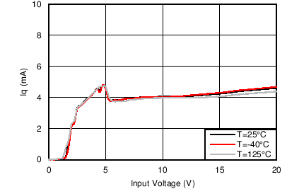
| Iq = IVDD + IA + IC + IOUTH | ||
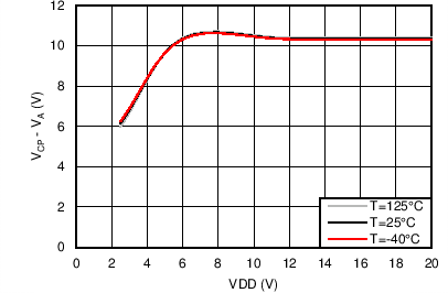
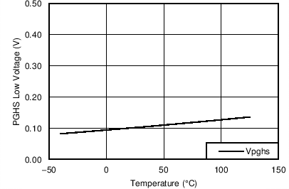
| IPGHS = 2mA | ||
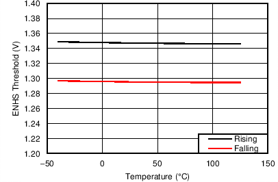
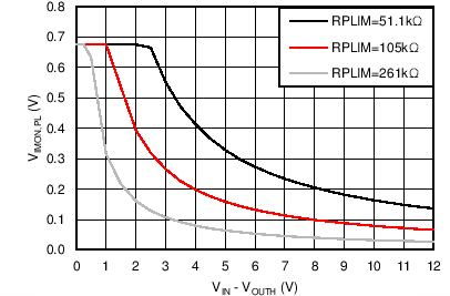
| VIMON during Power Limiting | ||
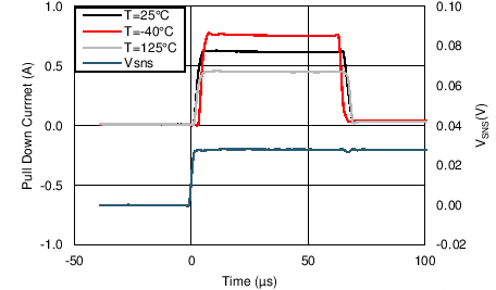
| VHGATE - VOUTH = 2V |
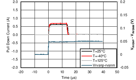
| VBGATE - VA = 4V | ||
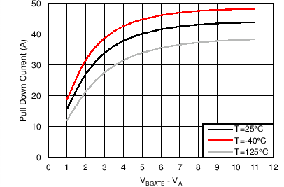
| Sustained Sink Current |
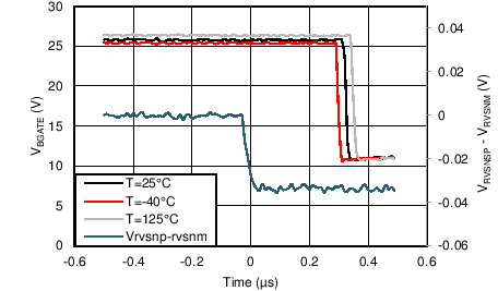
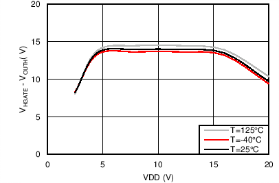
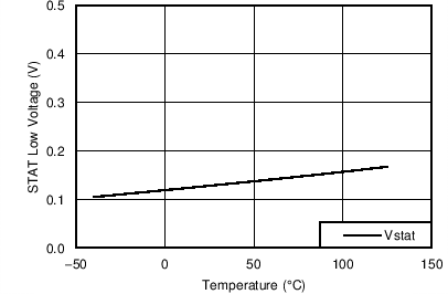
| ISTAT = 2mA | ||
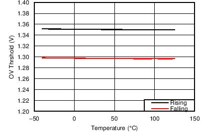
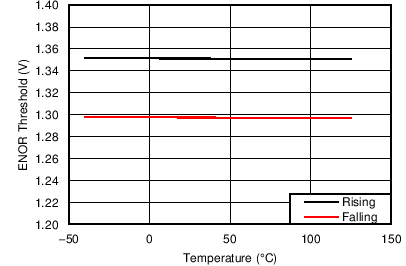
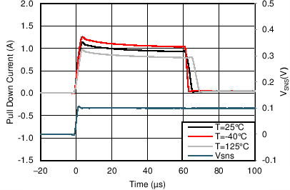
| VHGATE - VOUTH = 10V |
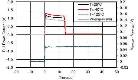
| VBGATE - VA = 10V | ||
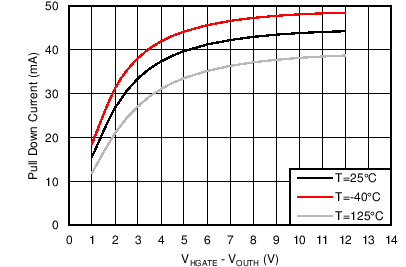
| Sustained Sink Current |
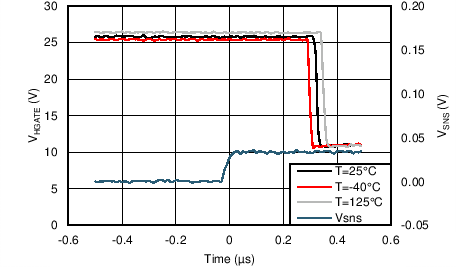
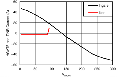
| VHGATE-OUTH =4V |