SLVSCV6A January 2015 – February 2015 TPS24740 , TPS24741 , TPS24742
PRODUCTION DATA.
- 1 Features
- 2 Applications
- 3 Description
- 4 Simplified Schematics
- 5 Revision History
- 6 Device Comparison Table
- 7 Pin Configuration and Functions
- 8 Specifications
-
9 Detailed Description
- 9.1 Overview
- 9.2 Functional Block Diagram
- 9.3
Feature Description
- 9.3.1 Internal Power ORing of TPS24740
- 9.3.2 Enable and Over-voltage Protection
- 9.3.3 Current Limit and Power Limit During Start-up
- 9.3.4 Two Level Protection During Regular Operation
- 9.3.5 Dual Timer (TFLT and TINR)
- 9.3.6 Using SoftStart - IHGATE and TINR Considerations
- 9.3.7 Three Options for Response to a Fast Trip
- 9.3.8 Programmable Reverse Voltage Threshold
- 9.3.9 Analog Current Monitor
- 9.3.10 Power Good Flag
- 9.3.11 ORing MOSFET Status Indicator
- 9.3.12 Fault Reporting
- 9.4 Device Functional Modes
-
10Application and Implementation
- 10.1 Application Information
- 10.2
Typical Application
- 10.2.1 30A Single channel OR then Hot Swap With Current Monitoring
- 10.2.2 Design Requirements
- 10.2.3
Detailed Design Procedure
- 10.2.3.1 Select RSNS and VSNS,CL Setting
- 10.2.3.2 Selecting the Fast Trip Threshold and Filtering
- 10.2.3.3 Selecting the Hot Swap FET(s)
- 10.2.3.4 Select Power Limit
- 10.2.3.5 Set Fault Timer
- 10.2.3.6 Check MOSFET SOA
- 10.2.3.7 Choose ORing MOSFET
- 10.2.3.8 Choose Reverse Current Threshold and Filtering
- 10.2.3.9 Choose Under Voltage and Over Voltage Settings
- 10.2.3.10 Selecting CIN, COUT, and CMIDDLE
- 10.2.3.11 Selecting D1 and D2
- 10.2.3.12 Ensuring Stability
- 10.2.3.13 Compute Tolerances
- 10.2.4 Application Curves
- 10.2.5
40 A Single Channel Hot Swap then ORing
- 10.2.5.1 Design Requirements
- 10.2.5.2
Design Procedure
- 10.2.5.2.1 Select RSNS and VSNS,CL Setting
- 10.2.5.2.2 Selecting the Fast Trip Threshold and Filtering
- 10.2.5.2.3 Selecting the Hot Swap FET
- 10.2.5.2.4 Select Power Limit
- 10.2.5.2.5 Set Fault Timer
- 10.2.5.2.6 Check MOSFET SOA
- 10.2.5.2.7 Checking Stability of Hot Swap Loop
- 10.2.5.2.8 Choose ORing MOSFET
- 10.2.5.2.9 Choose Reverse Current Threshold and Filtering
- 10.2.5.2.10 Choose Under Voltage and Over Voltage Settings
- 10.2.5.2.11 Selecting CIN, COUT, CMIDDLE, and Transient Protection
- 10.2.5.2.12 Adding CENHS
- 10.2.5.3 Application Curves
- 10.3 System Examples
- 11Power Supply Recommendations
- 12Layout
- 13Device and Documentation Support
- 14Mechanical, Packaging, and Orderable Information
Package Options
Mechanical Data (Package|Pins)
- RGE|24
Thermal pad, mechanical data (Package|Pins)
- RGE|24
Orderable Information
10 Application and Implementation
NOTE
Information in the following applications sections is not part of the TI component specification, and TI does not warrant its accuracy or completeness. TI’s customers are responsible for determining suitability of components for their purposes. Customers should validate and test their design implementation to confirm system functionality.
10.1 Application Information
The TPS2474x controls an ORing MOSFET and a Hot Swap MOSFET to provide complete protection in redundant systems. The two sections are mostly independent and the Hot Swap and ORing settings can be chosen independently. In addition the TPS2474x supports various system level configurations shown in System Examples. Since the ORing and Hot Swap control are independent the design procedure shown in the Typical Application section can be used for these different configurations as well. Note that the component selection can often be iterative; and, it is recommended to use the publically available excel calculators to crunch the numbers. See Tools & Software link on the Product folder.
10.2 Typical Application
Two application examples are provided. The first one is an OR then Hot Swap 30A design with a current monitoring requirement, which uses the TPS24740. The second design is a Hot Swap then ORing 40A design with a transient load requirement and a large output capacitor that uses the TPS24742. Note that there are a lot of calculations necessary for these designs and it is easy to make mistakes. For this reason it is recommended to use TI design calculators, which follow a very similar procedure. See Tools & Software link on the Product folder. These written examples should be used as reference to better understand the calculations implemented in the design calculators.
10.2.1 30A Single channel OR then Hot Swap With Current Monitoring
Figure 30 shows the application schematic for a single channel OR then Hot Swap configuration.
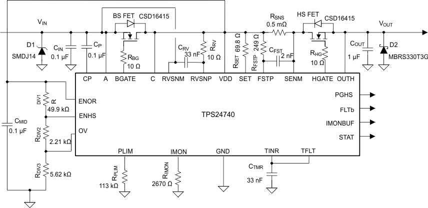 Figure 30. Application Schematic for ORing then Hot Swap
10.2.2 Design Requirements
Table 2 summarizes the design parameters that must be known before designing a Hot Swap circuit. When charging the output capacitor through the Hot Swap MOSFET, the FET’s total energy dissipation equals the total energy stored in the output capacitor (1/2CV2). Thus both the input voltage and output capacitance determines the stress experienced by the MOSFET. The maximum load current drives the current limit and sense resistor selection. In addition, the maximum load current, maximum ambient temperature, and the thermal properties of the PCB (RθCA) drives the selection of the MOSFET RDSON and the number of MOSFETs used. RθCA is a strong function of the layout and the amount of copper that is connected to the drain of the MOSFET. Air cooling also reduces RθCA. It is also important to know if there are any transient load requirements. Finally, whether current monitoring is needed and its accuracy requirement drives the selection of RSNS, RIMON, and RSET.
Table 2. Design Requirements for 30A ORing then Hot Swap
| DESIGN PARAMETER | EXAMPLE VALUE |
|---|---|
| Input voltage range | 11 V – 13 V |
| Maximum DC load current | 30A |
| Maximum Output Capacitance of the Hot Swap | 1500 µF |
| Maximum Ambient Temperature | 55°C |
| Minimum Ambient Temperature | 0°C |
| MOSFET RθCA (function of layout) | 30°C/W |
| Transient load requirement | No |
| Pass “Hot-Short” on Output? | Yes |
| Pass a “Start into short”? | Yes |
| Is the load off until PG asserted? | Yes |
| Current Monitoring Required (accuracy?) | Yes (<2.5% full scale) |
| IC used | TPS24740 |
10.2.3 Detailed Design Procedure
10.2.3.1 Select RSNS and VSNS,CL Setting
TPS2474x has a programmable VSNS,CL with a recommended range of 10 mV to 67.5 mV. It can be used with a VSNS,CL up to 200 mV, but that requires a resistor (RSTBL) between SET and SENM to ensure stability of an internal loop. RSTBL should be set larger than RIMON x RSET / (10xRSET- RIMON). This is shown in Figure 31.
For the majority of applications 25mV (RSTBL is not needed) is a good starting target for VSNS,CL. Targeting a current limit of 35A to allow margin for the load, the sense resistor can be calculated as follows

Since 0.71 mΩ resistors aren’t available, the closest standard resistor should be chosen. To have better efficiency, a 0.5 mΩ resistor is chosen. Next the VSNS,CL should be computed based on the actual RSNS and then used to compute RSET and RIMON. RSET is chosen to target 250 µA of current through SET and IMON pins during current limit.


Choose RSET to equal 69.8Ω, which is the closest available standard resistor. Next obtain the calculated RIMON (RIMON,CLC) as follows:

Choose 2.67kΩ resistor for RIMON, which is the closest available standard resistor. Since precision current monitoring is desired, 0.1% resistors were used for RIMON and for RSET and a 4 terminal sense resistor (WSL4026L5000) was used for RSNS.


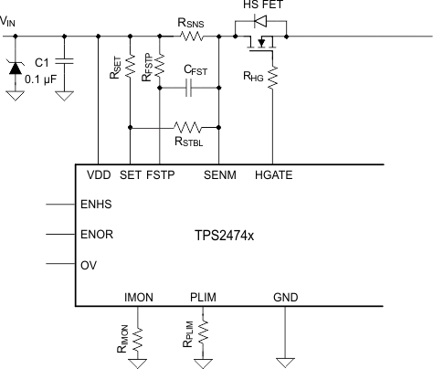 Figure 31. Adding RSTBL for VSNS,CL > 67.5mV
10.2.3.2 Selecting the Fast Trip Threshold and Filtering
The TPS2474x allows the user to program the fast trip threshold. When this threshold is exceeded the gate is quickly pulled down. CFSTP can be added to include some filtering into the comparator. The selection of the fast trip threshold and filtering is influenced by the systems environment and requirements. In general picking a larger threshold and larger filtering time will result in more immunity to nuisance trips, but also a slower response (possibly inadequate) to real fault conditions. It’s best to fine tune these threshold after testing the real system. As a starting point it is recommended to set the fast trip threshold at least 1.25x larger than then current limit. For this design example a 50A fast trip threshold along with a 500ns filtering time constant were targeted. The value for RFSTP and CFSTP can be computed as shown below:


The next closest standard resistor and capacitor values should be chosen. In this case RFSTP = 249Ω and CFSTP=2nF.
10.2.3.3 Selecting the Hot Swap FET(s)
It is critical to select the correct MOSFET for a Hot Swap design. The device must meet the following requirements:
- The VDS rating should be sufficient to handle the maximum system voltage along with any ringing caused by transients. For most 12V systems a 25 V or 30V FET is a good choice.
- The SOA of the FET should be sufficient to handle all usage cases: start-up, hot-short, start into short.
- RDSON should be sufficiently low to maintain the junction and case temperature below the maximum rating of the FET. In fact, it is recommended to keep the steady state FET temperature below 125°C to allow margin to handle transients.
- Maximum continuous current rating should be above the maximum load current and the pulsed drain current must be greater than the current threshold of the circuit breaker. Most MOSFETs that pass the first three requirements will also pass these two.
- A VGS rating of +16 V is required, because the TPS2474x can pull up the gate as high as 15.5 V above source.
For this design the CSD16415Q was selected for its low RDSON and superior SOA. After selecting the MOSFET, the maximum steady state case temperature can be computed as follows:

Note that the RDSON is a strong function of junction temperature, which for most MOSFETS will be very close to the case temperature. A few iterations of the above equations may be necessary to converge on the final RDSON and TC,MAX value. According to the CSD16415Q datasheet, its RDSON is about 1.3x greater at 100°C compared to room temperature. The equation below uses this RDSON value to compute the TC,MAX. Note that the computed TC,MAX is close to the junction temperature assumed for RDSON. Thus no further iterations are necessary.

10.2.3.4 Select Power Limit
In general, a lower power limit setting is preferred to reduce the stress on the MOSFET. However, at low power limit levels both the VSNS and VIMON become very low, which results in more error caused by offsets. It is recommended to keep VSNS above 1.5mV and VIMON above 27mV to ensure reasonable accuracy of the power limit engine. Based on these requirements the minimum power limit can be computed as seen in Equation 20.

In most applications the power limit can be set to PLIM,MIN using Equation 21. Here RSNS and RPWR are in Ωs and PLIM is in Watts.

The closest available resistor should be selected. In this case it is a 113 kΩ.
10.2.3.5 Set Fault Timer
The inrush timer runs when the Hot Swap is in power limit or current limit, which is the case during start-up. Thus the timer has to be sized large enough to prevent a time-out during start-up. If the part starts directly into current limit (ILIM × VIN < PLIM) the maximum start time can be computed with Equation 22:

For most designs (including this example) ILIM × VIN > PLIM so the Hot Swap will start in power limit and transition into current limit. In that case the maximum start time can be computed as seen in Equation 23:

Note that the above start-time is based on typical current limit and power limit values. To ensure that the timer never times out during start-up it is recommended to set the fault time (TINR) to be 1.5x tstart,max or 4.9 ms. This will account for the variation in power limit, timer current, and timer capacitance.
Next the design should decide if having equal TINR and TFLT is acceptable. If there is no transient load requirement this is usually fine. For this example the same capacitor is connected to both TINR and TFLT to save on BOM cost. In this case the time out (TTMR) should be set based on the TINR requirements. When these pins are connected the CTMR can be computed as follows:
The next largest available CTMR is chosen as 33nF. Once the CTMR is chosen the actual programmed time out can be computed as seen in Equation 25.

10.2.3.6 Check MOSFET SOA
Once the power limit and fault timer are chosen, it is critical to check that the FET remains within its SOA during all test conditions. For this design example the TPS24740 is used, which retries once during a hot-short.
During a “Hot-Short” the circuit breaker trips and the TPS24740 re-starts into power limit until the timer runs out. In the worst case the MOSFET’s VDS will equal VIN,MAX, IDS will equal PLIM / VIN,MAX and the stress event will last for TTMR. For this design example the MOSFET will have 13 V, 3 A across it for 5.6 ms.
Based on the SOA of the CSD16415Q, it can handle 13 V, 100 A for 1 ms and it can handle 13 V, 15 A for 10 ms. The SOA for 5.6 ms can be extrapolated by approximating SOA vs time as a power function as shown in Equation 26:
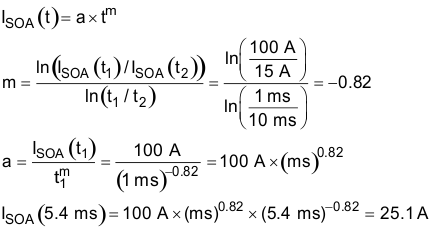
Note that the SOA of a MOSFET is specified at a case temperature of 25°C, while the case temperature can be much hotter during a hot-short. The SOA should be de-rated based on TC,MAX using Equation 27:

Based on this calculation the MOSFET can handle 11.67 A, 13 V for 5.6 ms at elevated case temperature, but is only required to handle 3A (39 W / 13 V) during a hot-short. Thus there is good margin and this will be a robust design. In general, it is recommended that the MOSFET can handle 1.3x more than what is required during a hot-short. This provides margin to cover the variance of the power limit and fault time.
10.2.3.7 Choose ORing MOSFET
When selecting the ORing MOSFET the considerations are similar to the Hot Swap MOSFET, but the SOA is no longer critical. In addition the lower RDSON is not always ideal, because that would result in a larger reverse current for the same reverse voltage threshold. Of course a lower RDSON would provide better efficiency. For consistency sake a single CSD16415Q FET was used for the ORing section as well. It is important to check its steady state temperature at max load using the same equation that was used for the Hot Swap.

10.2.3.8 Choose Reverse Current Threshold and Filtering
When setting the reverse current threshold, it is often desired to set a very low value to minimize the maximum DC reverse current. However, the accuracy of the reverse voltage threshold should be considered. The TPS2474x has a 1mV offset on the reverse voltage comparator. Thus setting a very low reverse voltage setting can result in some boards to trip at positive current. This would lead to oscillations at zero load condition as the ORing gate turns ON and OFF, which is typically not desired. Note that applications that always have a significant forward current will not experience this problem.
For this design example a reverse voltage of 1.5mV was targeted to keep the threshold low, but to also ensure that the device never trips at positive current. Just like the filtering on the fast trip threshold for the Hot Swap, the optimum time constant for filtering the reverse voltage threshold will depend on the system environment and requirements. Again, this is a trade-off between avoiding nuisance trips and a fast response to actual faults. In general a 500ns time constant is a good starting point. Based on these target thresholds, RRV and CRV can be computed using Equation 29 and Equation 30.


Choose closest available standards values: RRV = 15Ω and CRV = 33nF.
10.2.3.9 Choose Under Voltage and Over Voltage Settings
The TPS2474x has comparators with 1.35V threshold on the ENHS, ENOR, and OV pins. A resistor divider can be used to set Undervoltage and Overvoltage thresholds for the bus. For this design example 10V and 14V were chosen as the limits to allow some margin for the 11V to 13V input bus. Once these limits are known, RDIV2 and RDIV3 can be computed using Equation 31, Equation 32, and Equation 33. RDIV1 was set to 49.9 kΩ, which keeps the power consumption reasonably low without being too susceptible to leakage currents.


Choose closest available standard 1% resistors: RDIV2 = 2.21 kΩ and RDIV3 = 5.62 kΩ. The actual Under Voltage and Over Voltage settings can be computed for the chosen resistors as shown in Equation 34 and Equation 35:


10.2.3.10 Selecting CIN, COUT, and CMIDDLE
It is recommended to add ceramic bypass capacitors to help stabilize the voltages on the input, output, and the intermediate node. Since CIN and CMIDDLE will be charged directly on hot-plug, their value should be kept small. 0.1µF is a good target. Since COUT doesn’t get charged during hot-plug, a larger value such as 1 µF could be used.
10.2.3.11 Selecting D1 and D2
During hot plug and hot short events there could be significant transients on the input and output of the hotswap that could cause operation outside of the IC specifications. To ensure reliable operation a TVS on the input and a Schottky diode on the output are recommended. In this example a SMDJ14A and MBRS330T3G are used.
10.2.3.12 Ensuring Stability
For most applications, the TPS2474x is stable whithout any additional components. However in some cases additional CGS,EXT is required as shown in Figure 32 to help stabilize the current and power limit loop. Typically this is for low current limits and low sense voltages. It is easy to check whether these extra components are needed using the equations below. Note that the transconductance ( also referred to as gm and gfs) of the FET will vary based on the current and thus gm' is used in the equations as a normalizing parameter. The CSD16415 has a gm of 168 siemens at 40A of IDS, resulting in gm' of 26.56. For this example, CGS,MIN was computed to be 0.9nF, while the CISS of the CSD16415 is 3.15nF providing plenty of margin for the design. In general it is recommended to have a 2x margin from the typical CISS and CGS,MIN to account for any variation that the FET would have. If the CISS of the MOSFET isn't large enough an external RC should be added as shown in the figure below. Note that if parallel FETs are used CGS,MIN (per FET) is reduced by square root of two or by 1.41.


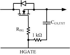 Figure 32. Ensuring Stability
10.2.3.13 Compute Tolerances
After finishing a design it is often desired to know the variations of each setting. Often times there are multiple error sources and there are two common ways to analyze the circuit. One is worst case, which adds all of the error sources. The other one is root mean square (RMS), which is less conservative. When error sources are independent using the RMS method provides a more statistically accurate view of the tolerances. This method is used in this section. Note that the error calculations are quite long and tedious and it is recommended to use TI’s excel tools, which support both worst case and RMS analysis. For this example the tolerances in Table 3 are assumed. See Tools & Software link on the Product folder.
Table 3. Component Tolerances
| COMPONENTS | TOLERANCE |
|---|---|
| RIMON and RSET | 0.1% |
| RSNS | 1% |
| RDIV1, RDIV2, RDIV3, RPLIM, RFST, | 1% |
| CTMR | 10% |
First, the tolerance of the current monitoring and current limit is computed.
There are 5 error sourcing contributing to the current monitoring accuracy on the IMON pin: tolerance of RSET (ERSET), tolerance of RIMON (ERIMON), tolerance of RSNS (ERSNS), the IC gain error (ERGAIN), and the IC offset error (EROS). All of these errors are in % with the exception of the offset error. To get a percent error due to the offset error (EROS%) simply divide the offset by the sense voltage. For the TPS2474x, ERGAIN is 0.4%, and EROS is 150 µV.
Based on these values the full scale (IFS,ERR,IMON) and 20% of full scale (I20FS,ERR,IMON) current monitoring accuracy at the Imon pin can be computed with Equation 39 and Equation 40.


Note that the TPS24740 detects the current limit when the IMON pin exceeds 675 mV. Thus the current limit error ILIM,ER is a combination of the IFS,ERR,IMON and the current limit error at the IMON pin (ILIM,ERR,IMON). The 675 mV threshold varies up to 15 mV so ILIM,ERR,IMON is 2.3% and the current limit error can be computed as seen in Equation 41:

If the current is monitored at the IMONBUF pin, there is additional error introduced due to the internal buffer, which has a gain error of 0.66% (EROS,BUF) and an offset error of 3mV (EROS,BUF) referred to the IMON pin. Note that VIMON equals 675 mV at full scale and 135 mV at 20% of full scale. Thus the total current monitoring error at the IMONBUF pin for full scale (IFS,ERR,IMONBUF) and 20% of full scale (I20FS,ERR,IMONBUF) can be found using Equation 42 and Equation 43 :


Next the power limit error is computed. This error is made up of three sources: the error from external components (ERRCOMP), the error when translating the sense voltage to IMON (IPL,ERR,IMON), and the error of the power limit engine at IMON (ERRIMON,PL). Both ERRSNS and ERRIMON, PL are a function of the operating point of the power limit engine. Note that this error is greatest at largest VDS, since VSNS,PL is smallest (refer to Figure 20). For this example VDS is largest when VIN = 13 V (maximum VIN) and VOUT = 0 V and thus the error is computed at this operating point. The sense voltage (VSNS) and the voltage at the IMON pin (VIMON) should be computed for this operating point using Equation 44 and Equation 45:


The IPL,ERR,IMON can be computed similarly to IFS,ERR,IMON using Equation 46.

The tolerance of the power limit engine is specified at three VIMON points in the datasheet: 135 mV (±20.3 mV), 67.5 mV (±10.1 mV), and 27 mV (±8.1 mV). To get the % error at the real operating point, the absolute error should be extrapolated and divided by VIMON as shown in Equation 47. This is graphically depicted in Figure 33.

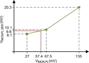 Figure 33. Extrapolating Power Limit Error
Once ERRIMON,PL and IPL,ERR,IMON are known the total power limit error (PLERR,TOT) can be computed using Equation 48. The component error comes from RSNS (1%), RPLIM (1%), RSET (0.1%), and RIMON (0.1%) resulting in a total component error of 1.4%.

After computing the fast trip voltage threshold to be 24.9 mV (100 µA × 249 Ω), the fast trip threshold error resulting from the IC (FSTERR, IC) can be computed using a similar extrapolation method as used for power limit. The component error of RSNS and RFST should be added to obtain the total fast trip error (FSTERR,TOT) showin in Equation 49 and Equation 50 below.


The IC error of the UV/OV threshold is always 3.7% (0.05 V/1.35 V). Assuming that all resistors have a 1% error the component error is 1.41% (2 resistors). When using the RMS method the total error is 4%. For the timer error, the IC contributes 22% and 10% comes from the component. When using the RMS method the total error becomes 24.1%.
Table 4 summarizes the final tolerances of the design:
Table 4. Design Tolerances
| SETTINGS | ACCURACY |
|---|---|
| Current Limit | 2.7% |
| Fast Trip | 8.9% |
| Power Limit | 19.5% |
| Timer | 24.1% |
| UV/OV | 4.0% |
| Current Monitoring at IMON (Full Scale) | 1.4% |
| Current Monitoring at IMON (20% of Full Scale) | 4.4% |
| Current Monitoring at IMONBUF (Full Scale) | 1.6% |
| Current Monitoring at IMONBUF (20% of Full Scale) | 5.0% |
10.2.4 Application Curves
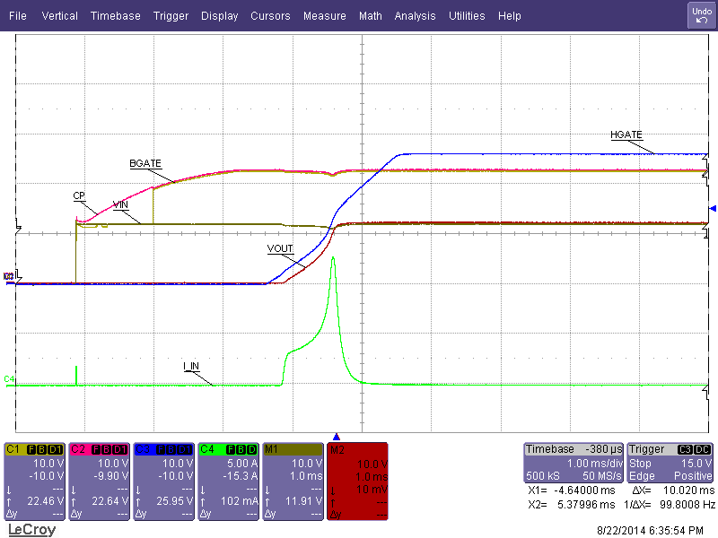 Figure 34. Start up (COUT= 440 µF)
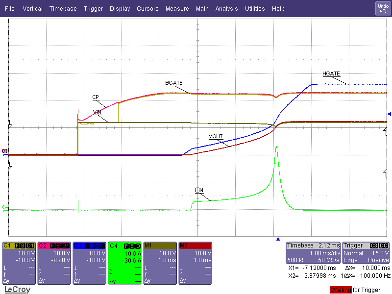 Figure 36. Start up (COUT=1500 µF)
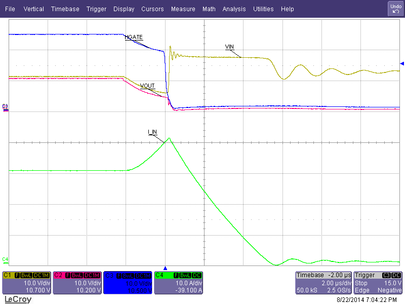 Figure 38. Hot Short on VOUT (zoomed in)
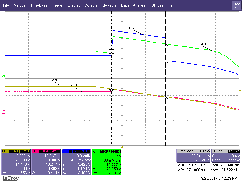 Figure 40. Under/Over Voltage with VIN Falling
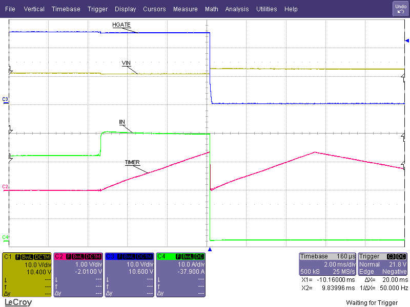 Figure 42. Load Step 32A to 40A
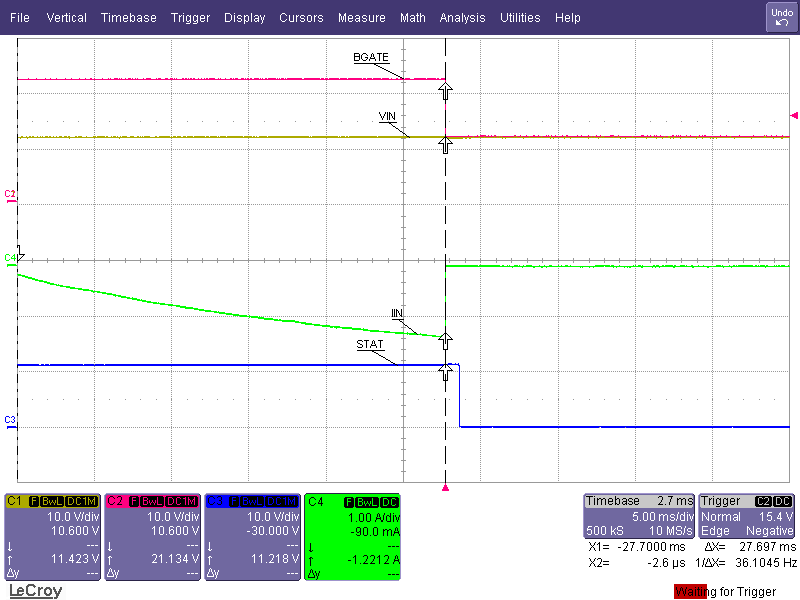 Figure 44. Gradual Reverse Current
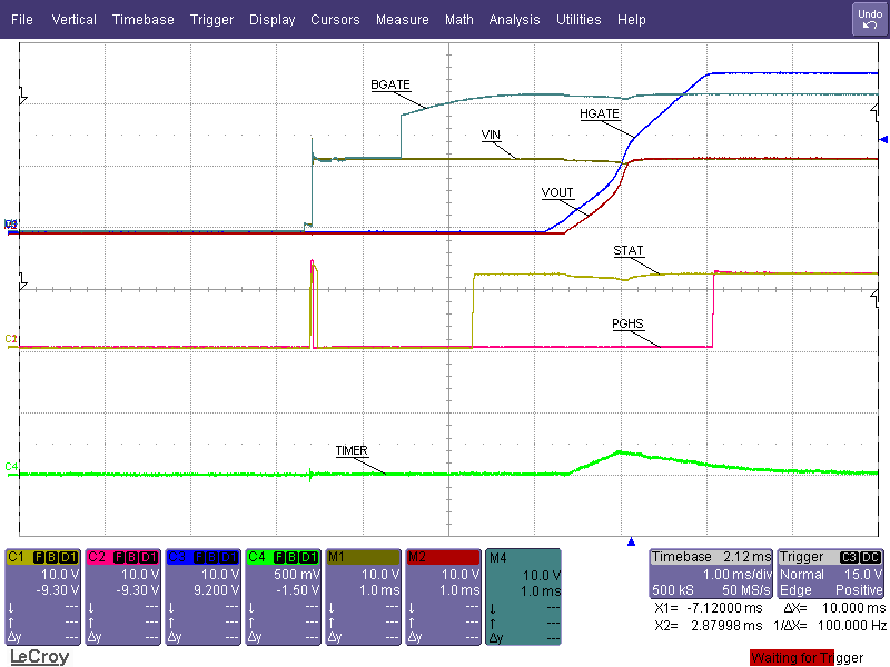 Figure 35. Start up (COUT= 440 µF)
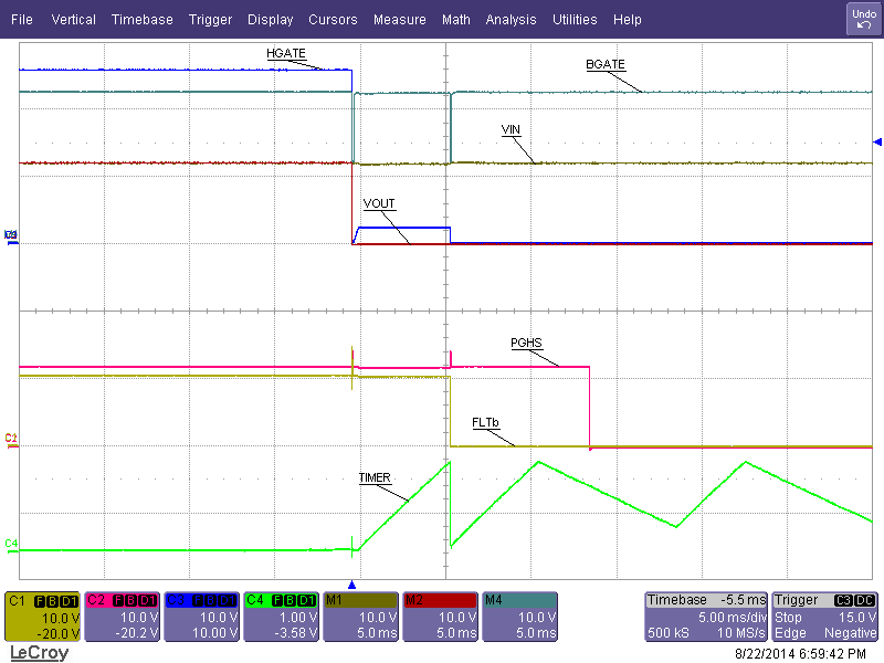 Figure 37. Hot Short on VOUT (zoomed out)
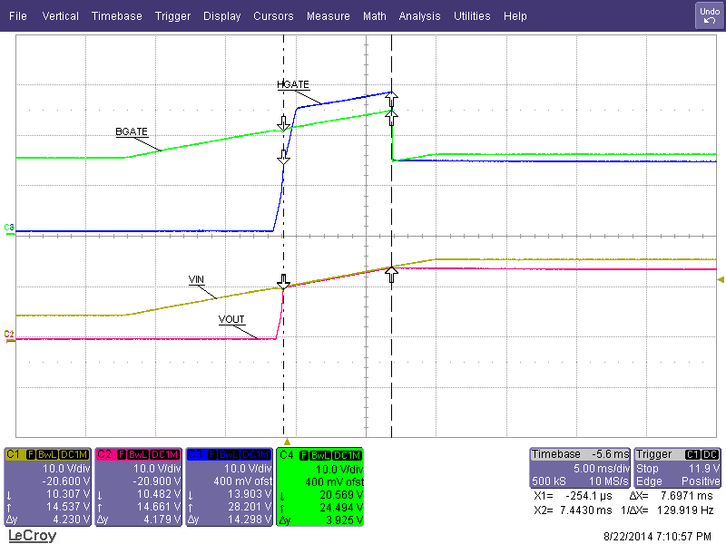 Figure 39. Under/Over Voltage with VIN Rising
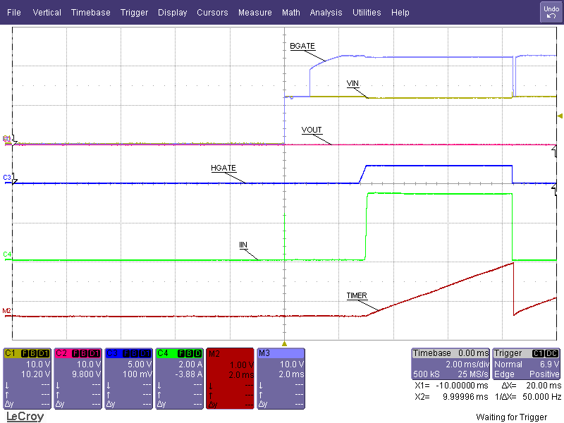 Figure 41. Start Up with VOUT Shorted
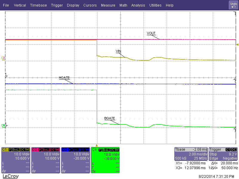 Figure 43. Hot – Short on VIN
10.2.5 40 A Single Channel Hot Swap then ORing
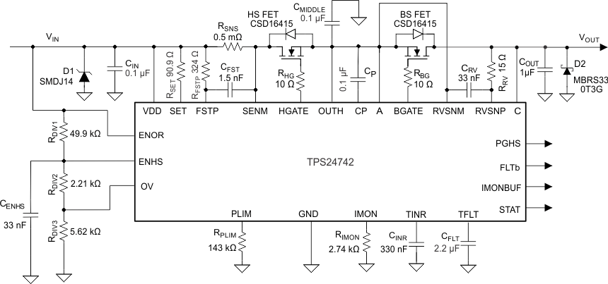 Figure 45. Application Schematic for Hot Swap then ORing
10.2.5.1 Design Requirements
This second design example is similar to the first one, but has a few key differences. First of all, the maximum output capacitance is much larger, and the maximum current is also larger, which puts more stress on the MOSFET. On the flip side, the TPS24742 IC is used, which results in less MOSFET stress during a hot-short event, because there is no restart. Finally, there is a requirement that the design should allow for 60A to pass through for 200 ms without shutting down. This requires the use of two timers. In addition, there is no requirement for accurate current monitoring and hence it’s not necessary to use a 4 terminal sense resistor.
Table 5. Design Requirements for 40A ORing then Hot Swap
| DESIGN PARAMETER | EXAMPLE VALUE |
|---|---|
| Input voltage range | 11 V – 13 V |
| Maximum DC load current | 40A |
| Maximum Output Capacitance of the Hot Swap | 10,000 µF |
| Maximum Ambient Temperature | 55°C |
| MOSFET RθCA (function of layout) | 30°C/W |
| Transient load requirement | Yes, 60A for 200ms |
| Pass “Hot-Short” on Output? | Yes |
| Pass a “Start into short”? | Yes |
| Is the load off until PG asserted? | Yes |
| IC used | TPS24742 |
| Current Monitoring Required | No |
| Can a hot board be unplugged and plugged back in? | No |
10.2.5.2 Design Procedure
10.2.5.2.1 Select RSNS and VSNS,CL Setting
Similarly to the previous design example, 25mV is used as a starting target for VSNS,CL. Targeting a current limit of 45A to allow margin for the load, the sense resistor can be computed as follows:

Since 0.55 mΩ resistors aren’t available, the closest standard resistor should be chosen. To have better efficiency, a 0.5 mΩ resistor is chosen. Next the VSNS,CL should be computed based on the actual RSNS and then used to compute RSET and RIMON. RSET is chosen to target 250 µA of current through SET and IMON pins during current limit.
Chose RSET to equal 90.9Ω, which is the closest available standard resistor. Next obtain the calculated RIMON (RIMON,CLC) as follows:

Choose 2.74kΩ resistor for RIMON, which is the closest available standard resistor. Since precision current monitoring is not needed 1% resistors were used for RIMON and for RSET and a 2 terminal sense resistor (HCS2512FTL500) was used for RSNS.
Finally, compute the actual current limit (ILIM,CL) :

10.2.5.2.2 Selecting the Fast Trip Threshold and Filtering
The TPS2474x allows the user to program the fast trip threshold. When this threshold is exceeded the gate is quickly pulled down. CFSTP can be added to include some filtering into the comparator. The selection of the fast trip threshold and filtering is influenced by the systems environment and requirements. In general picking a larger threshold and larger filtering time will result in more immunity to nuisance trips, but also a slower response (possibly inadequate) to real fault conditions. It’s best to fine tune these threshold after testing the real system. As a starting point it is recommended to set the fast trip threshold at least 1.25x larger than then current limit. For this design example a 65A fast trip threshold along with a 500ns filtering time constant were targeted to make sure that the 60A load transient can be passed. The value for RFSTP and CFSTP can be computed as shown in Equation 56 and Equation 57:


The next closest standard resistor and capacitor values should be chosen. In this case RFSTP = 324Ω and CFSTP=1.5nF.
10.2.5.2.3 Selecting the Hot Swap FET
It is critical to select the correct MOSFET for a Hot Swap design. The device must meet the following requirements:
- The VDS rating should be sufficient to handle the maximum system voltage along with any ringing caused by transients. For most 12V systems a 25 V or 30V FET is a good choice.
- The SOA of the FET should be sufficient to handle all usage cases: start-up, hot-short, start into short.
- RDSON should be sufficiently low to maintain the junction and case temperature below the maximum rating of the FET. In fact, it is recommended to keep the steady state FET temperature below 125°C to allow margin to handle transients.
- Maximum continuous current rating should be above the maximum load current and the pulsed drain current must be greater than the current threshold of the circuit breaker. Most MOSFETs that pass the first three requirements will also pass these two.
- A VGS rating of +16 V is required, because the TPS2474x can pull up the gate as high as 15.5 V above source.
For this design the CSD16415Q was selected for its low RDSON and superior SOA. After selecting the MOSFET, the maximum steady state case temperature can be computed as seen in Equation 58:

Note that the RDSON is a strong function of junction temperature, which for most MOSFETS will be very close to the case temperature. A few iterations of the above equations may be necessary to converge on the final RDSON and TC,MAX value. According to the CSD16415Q datasheet, its RDSON is about 1.4 × greater at 120°C compared to room temperature. Equation 59 uses this RDSON value to compute the TC,MAX. Note that the computed TC,MAX is close to the junction temperature assumed for RDSON. Thus no further iterations are necessary.

10.2.5.2.4 Select Power Limit
In general, a lower power limit setting is preferred to reduce the stress on the MOSFET. However, at low power limit levels both the VSNS and VIMON become very low, which results in more error caused by offsets. It is recommended to keep VSNS above 1.5mV and VIMON above 27mV to ensure reasonable accuracy of the power limit engine. Based on these requirements the minimum power limit can be computed as shown in Equation 60:

In most applications the power limit can be set to PLIM,MIN using the equation below. Here RSNS and RPWR are in Ωs and PLIM is in Watts.

The closest available resistor should be selected. In this case it is a 143 kΩ.
10.2.5.2.5 Set Fault Timer
The inrush timer runs when the Hot Swap is in power limit or current limit, which is the case during start-up. Thus the timer has to be sized large enough to prevent a time-out during start-up. If the part starts directly into current limit (ILIM × VIN < PLIM) the maximum start time can be computed with Equation 62:

For most designs (including this example) ILIM × VIN > PLIM so the Hot Swap will start in power limit and transition into current limit. In that case the maximum start time can be computed as seen in Equation 63:

Note that the above start time is based on typical current limit and power limit values. To ensure that the timer never times out during start-up it is recommended to set the fault time (TINR) to be 1.5x tstart,max or 32.6 ms. This will account for the variation in power limit, timer current, and timer capacitance.
Next the designer should decide if having equal TINR and TFLT is acceptable. Note that to pass the load transient the fault timer needs to be longer than 200 ms. If the inrush time is this long, it will place too much stress on the MOSFET during a start into short. For this reason, it’s ideal to have two separate timers. To ensure proper start up and to pass the load transient a target inrush time (TINR,TGT) of 32.6 ms and a target fault time (TFLT,TGT) of 250ms is used. CINR,CLC and CFLT,CLC is computed as seen in Equation 64 and Equation 65 :


The next largest available CINR is chosen as 330nF and the next largest available CFLT is chosen as 2.2µF
Next, the actual TINR and TFLT can be computed as shown below: Once CTMR and CFLT is chosen the actual programmed time out can be computed as shown in Equation 66 and Equation 67.


10.2.5.2.6 Check MOSFET SOA
Once the power limit and fault timer are chosen, it’s critical to check that the FET will stay within its SOA during all test conditions. For this design example the TPS24742 is used, which does not retry during a hot-short. Thus the worst condition is a start-up with output shorted to GND. In this case the TPS24742 will start into a power limit and regulate at that point for 43.5 ms (TINR). Based on the SOA of the CSD16415Q, it can handle 13 V, 15 A for 10 ms and it can handle 13 V, 4 A for 100 ms. The SOA for 43.5 ms can be extrapolated by approximating SOA vs time as a power function as shown in Equation 68:
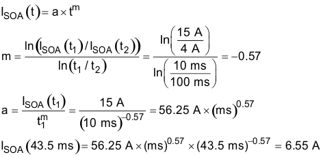
Note that the SOA of a MOSFET is specified at a case temperature of 25°C, while the case temperature can be hotter during a start into a short. It is important to understand the hottest temperature that a MOSFET can be during a start-up (TC, MAX, START). If a board has been off for a while and then it’s turned on TA, MAX is a good estimate for TC,MAX, START. However, if a board is on and then gets power cycled TC,MAX should be used for TC,MAX,START. This will depend on system requirements. For this design example it is assumed that the board can only be plugged in cold and TA,MAX is used to estimate TC,MAX,START.

Based on this calculation the MOSFET can handle 4.98 A, 13 V for 43.5 ms at 55°C elevated case temperature, but is only required to handle 3A during a hot-short. Thus there is good margin and this will be a robust design. In general, it is recommended that the MOSFET can handle 1.3x more than what is required during a worst case operating condition. This provides margin to cover the variance of the power limit and fault time.
10.2.5.2.7 Checking Stability of Hot Swap Loop
Using the same method as shown for the OR then Hot Swap example, Ensuring Stability, the minimum required CGS is computed to be 0.6 nF. Again the CISS is 3.1nF and there is plenty of margin to ensure stability.
10.2.5.2.8 Choose ORing MOSFET
When selecting the ORing MOSFET, the considerations are similar to the Hot Swap MOSFET, but the SOA is no longer critical. In addition the lower RDSON is not always ideal, because that would result in a larger reverse current for the same reverse voltage threshold. Of course a lower RDSON would provide better efficiency. For consistency sake a single CSD16415Q FET was used for the ORing section as well. It’s important to check its steady state temperature at max load using the same equation that was used for the Hot Swap.

10.2.5.2.9 Choose Reverse Current Threshold and Filtering
Same settings were used as the previous design example.
10.2.5.2.10 Choose Under Voltage and Over Voltage Settings
Same settings were used as the previous design example.
10.2.5.2.11 Selecting CIN, COUT, CMIDDLE, and Transient Protection
Same settings were used as the previous design example
10.2.5.2.12 Adding CENHS
When the ENHS pulled below its threshold and raised back up the IC will reset. Note that during a hot short the input voltage can easily droop below the UV threshold and cycle the ENHS pin. For the TPS24740 and TPS24741 IC’s this will not cause any issues. However, when using the TPS24742 the cycling of the ENHS will result in the IC attempting to restart, which is undesired (this is the main reason why someone would use the TPS24742). To avoid this behavior a capacitor should be added to the ENHS to provide filtering. For this example 33 nF was chosen.
10.2.5.3 Application Curves
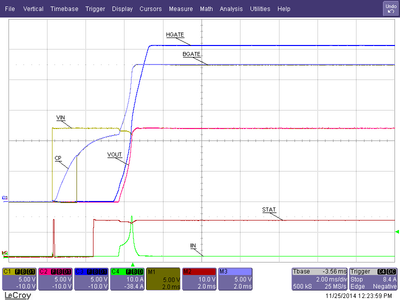 Figure 46. Start up (COUT=440µF)
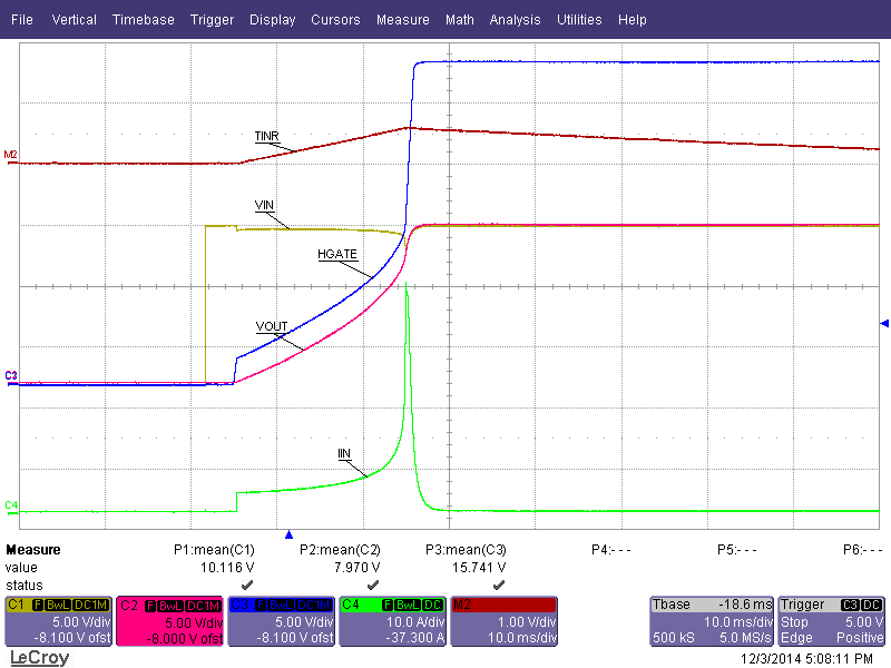 Figure 47. Start up (COUT=10,000µF, VIN = 13V)
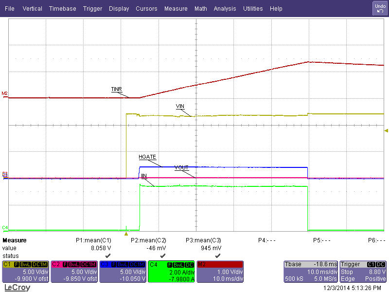 Figure 48. Start up Into Short on VOUT
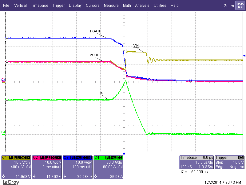 Figure 50. Hot – Short on VOUT(zoomed in)
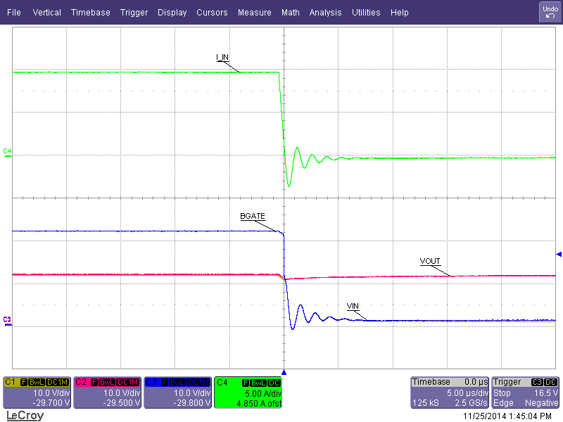 Figure 52. Short Vin (ILOAD = 10A)
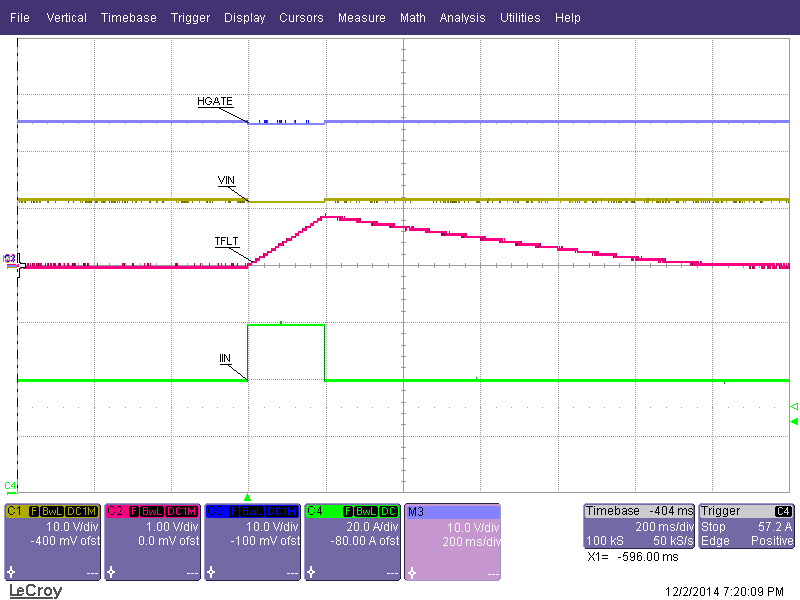 Figure 54. 60A Load Step for 200 ms
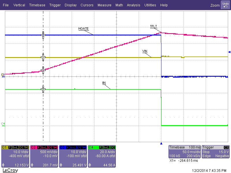 Figure 56. Gradual Overcurrent
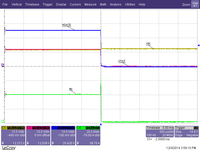 Figure 49. Hot Short on VOUT
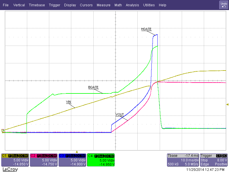 Figure 51. Under/Over Voltage with VIN Rising
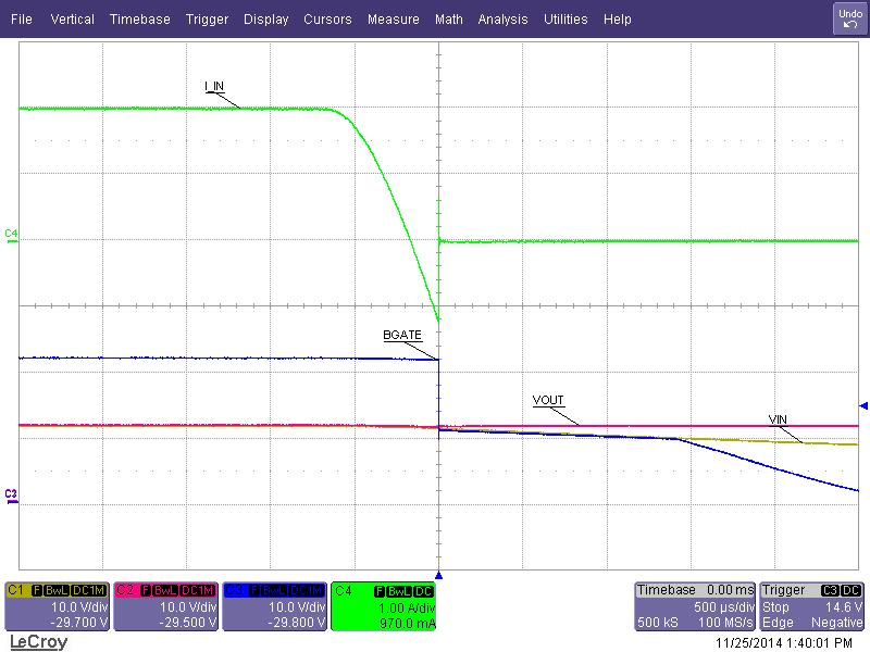 Figure 53. Gradual Reverse Current
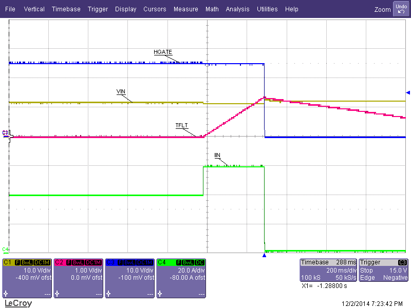 Figure 55. Load Step 40A to 60A
10.3 System Examples
The TPS2474x is a flexible Hot Swap and ORing controller that can supports many redundant configurations. The following section goes through the various system level configurations and the advantages of each one. It also shows how the TPS2474x will behave under system level tests.
10.3.1 TPS2474x in Battery Back Up
Some battery back-up units are set up to support both charging and discharging from the same terminal. In this case a configuration shown in Figure 57 can be used. In normal operation the load is power from the AC/DC, while the BBU is charged from the mid-point. The Hot Swap will provide inrush and fault protection to the load. If the AC/DC fails the ORing will prevent the reverse current to the AC/DC and the load will get powered from the BBU.
 Figure 57. Block Diagram for Hot Swap and ORing in BBU Applications
Figure 58 shows the schematic for this implementation. It is important to connect VDD to the mid-point to ensure that the IC has power even if VIN goes away. In addition the ENHS pin should be based on the mid-point voltage to ensure that the Hot Swap stays ON even if the VIN power goes away.
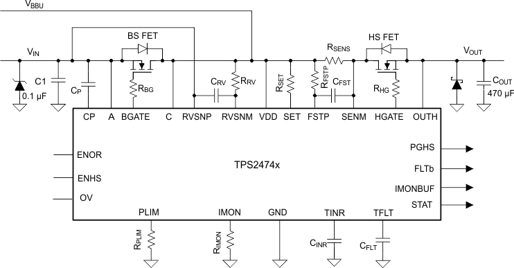 Figure 58. Application Schematic for TPS2474x in BBU Applications
Figure 59 shows a switch over from the AC/DC power (VIN) to BBU power with a 12A load. The BBU is modeled as drawing 4A when VMIDDLE > 12V and supplying up to 20A when VMIDDLE < 12V. Note that when VIN collapses the BBU current goes from negative to positive and the BGATE goes down to prevent the AC/DC from draining power from the BBU.
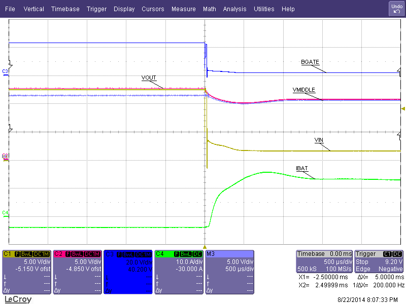 Figure 59. Switch Over to Battery Power
10.3.2 TPS2474x in Priority Muxing
Priority muxing is used in the following scenario:
- The system should be powered from Main when it’s present
- The system should be powered from Auxiliary when Main goes away.
- Auxiliary voltage may be above the Main voltage.
- The system should support a short to ground on both Main and Aux.
Due to condition 3, the 2 supplies can’t be simply ORed together because the load could start drawing power from AUX. That’s why an additional Hot Swap is required on the AUX rail to prevent the forward current flow. The OV pin of the TPS2474x can be used to keep the Auxiliary Hot Swap OFF unless the voltage on MAIN falls below a certain threshold.
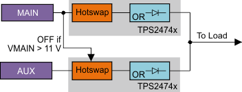 Figure 60. Block Diagram for Priority Muxing
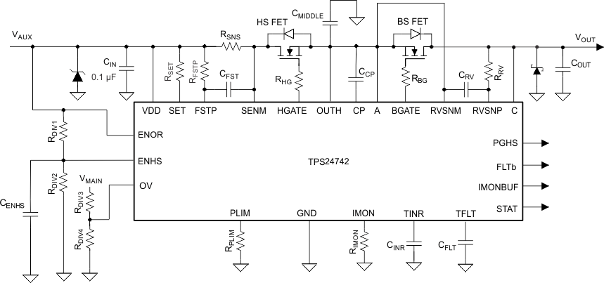 Figure 61. OV Pin Hook Up on the AUX Channel
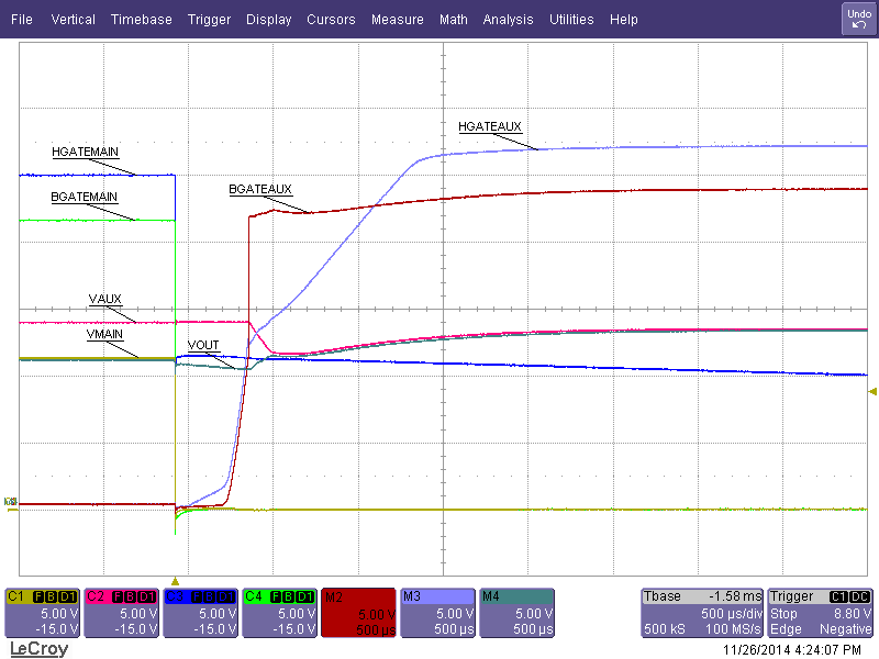
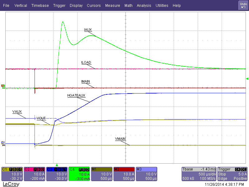
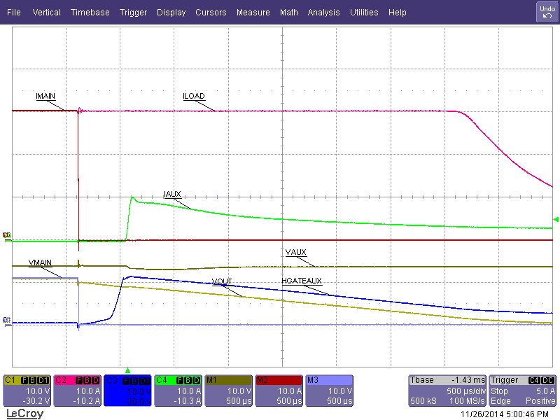
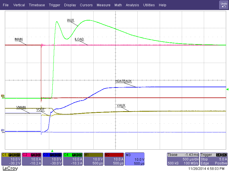
The following waveforms show the performance of the priority mux using the settings from the Hot Swap then ORing design example. The OV pin on the AUX side was set to make it turn on once Main was below 11V. Note that for a 10A load the switch over occurs without any issues, but the system cannot handle it at 30A. This occurs due to VAUX being higher than VMAIN and VOUT drooping after the main channel shuts down and the AUX channel coming back up. As a result there is a voltage drop across the Hot Swap MOSFET (VAUX – VOUT) and the TPS24742 limits the input current to PLIM/VDS. If the supplied current is lower than the load current the output capacitor continues to discharge and the system shuts down. When the power limit was increased to 160W the switch over occurred without any issues, because sufficient current was supplied to power the load and charge the output capacitor.
 |
 |
|
|
Figure 62. Switch from Main to Aux (VMAIN = 12V, VAUX = 14V, ILOAD = 10A)
|
||
|
|
|||||||
|
Figure 63. Switch from Main to Aux with VMAIN = 12V, VAUX = 14V, ILOAD = 30A
(left: PLIM = 39W, right; PLIM = 160W) |
||||||||
10.3.3 TPS2474x with Multiple Loads and Multiple Supplies
Figure 64 applies to systems that have multiple supplies and multiple loads. The ORing after each supply ensures that the loads won’t lose power if any of the supplies fail and the Hot Swap in front of each load ensures that a failure on one load doesn’t affect the operation of the other loads. The node on the output of ORing and input of the Hot Swaps is referred to as VMIDDLE.
 Figure 64. Block Diagram for Systems with Multiple Supplies and Loads
Figure 65 shows a hot-short on load 1, which results in a shutdown of the first Hot Swap gate. Note that the second load continues to be powered as both HGATE2 and VMIDDLE stay high.
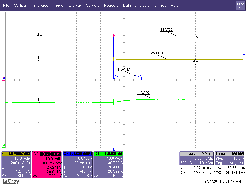 Figure 65. Hot Short on Load 1, Load 2 Not Interrupted
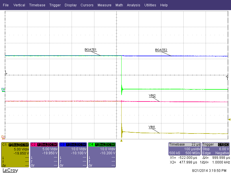
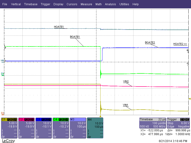
The main purpose of the ORing controller is to protect the loads when one of the input supplies has a failure. The two waveforms below show this scenario. The left waveform shows a condition where both of the power supplies are at the same voltage and both of the BGATEs are ON. When VIN1 goes to ground BGATE1 quickly turns OFF, while BGATE2 remains ON. In the waveform on the right VIN1 is above VIN2 so the system starts by with only BGATE1 being ON. When VIN1 goes to ground, BGATE1 quickly turns off and BGATE2 turns ON. There is a short delay between BGATE1 turning off and BGATE2 turning ON. This pause is due to VMIDDLE discharging from 12.5V to 12V (BGATE2 will only turn on when VIN2 > VMIDDLE)
|
|
|||||||
|
Figure 66. Hot Short on VIN1
(left: VIN1 = VIN2 = 12V; right VIN1 =12.5V, VIN2 = 12V, ILOAD1 = ILOAD2 = 12A ) |
||||||||
Figure 67 shows a system configuration where VIN1 equals VIN2 and VIN2 is hot plugged. Note that when BGATE2 comes up almost immediately and VIN1 raises as well. This is due to the fact that VIN1 had some voltage droop due to the IR drop of the input impedance. When a second supply was placed in parallel the load was shared reducing the droop. The quick input spike on VIN2 is due input inductance.
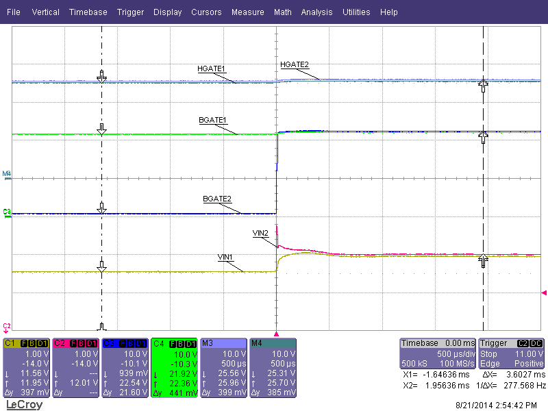 Figure 67. Hot Plug VIN2 (VIN1 = 12V; VIN2 = 12V; ILOAD1 = ILOAD2 = 12A)
10.3.4 Two Supplies Powering a Load
Figure 68 can be used when ORing two power supplies together to drive a single load. The ORing provide protection in case one of the AC/DC’s fail and the Hot Swap provides protection if there is a failure at the load and if one of the AC/DC output voltages has an overvoltage condition.
 Figure 68. Block Diagram for ORing Two Power Supplies
Figure 69 and Figure 70 shows a hot plug event on power supply A, when power supply B is already up. If VINA is above VINB, the blocking gate of channel B turns off and the load is powered from channel A. If VINA is below VINB, BGATEA doesn’t enhance and the power continues to be supplied from channel B.
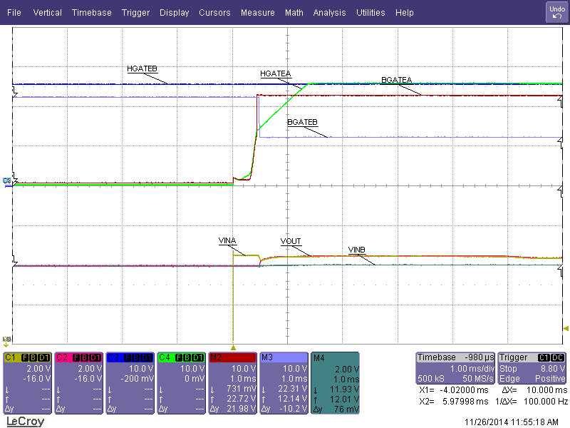 Figure 69. Hot Plug VINA (VINA =12.5, VINB = 12V, RLOAD = 10Ω)
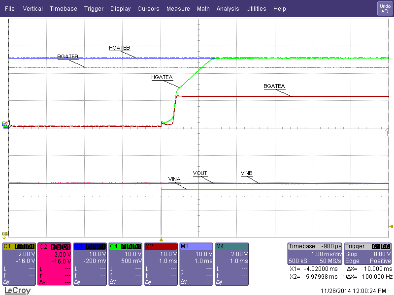 Figure 70. Hot Plug VINA (VINA =11.5V, VIN2 = 12V, RLOAD = 10Ω)
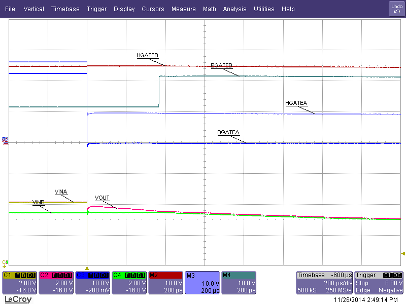
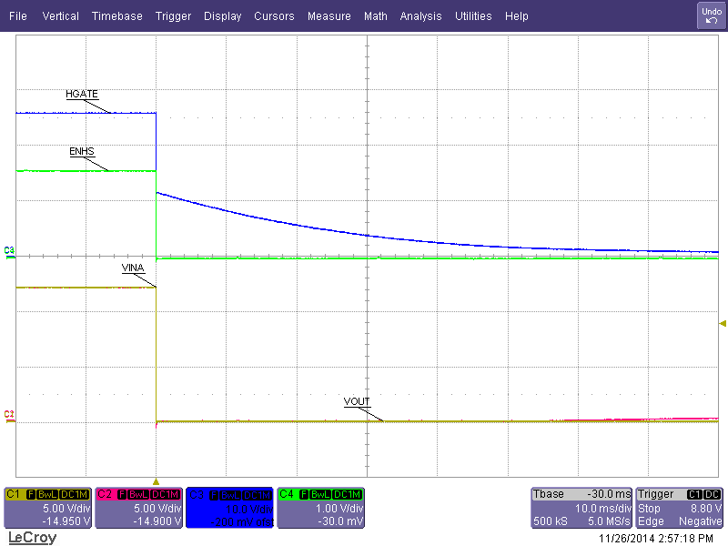
Figure 71 shows power switching from VINA to VINB after VINA shorts to ground. Note that VOUT droops until it is at the same level as VINB when BGATEB turns on.
 |
 |
|
|
Figure 71. Short on VINA Zoomed In and Zoomed Out View (ILOAD=10A, VINA = 12V, VINB = 11.5V)
|
||
Figure 72 shows the same event when VINA and VINB are equal and both channels are on before VINA shorts to ground. Note channel B stays on and channel A shuts down.
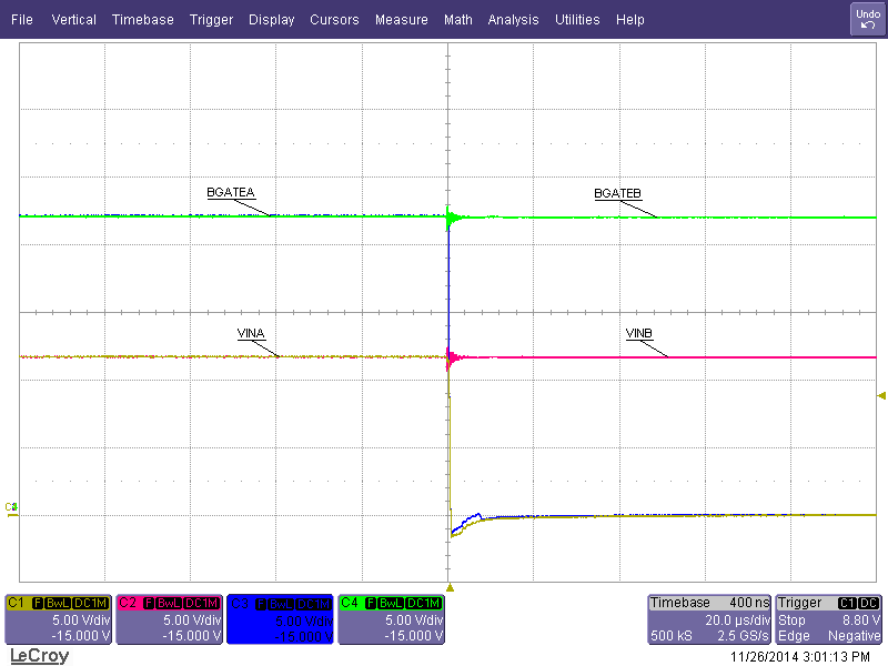 Figure 72. Short on VINA (ILOAD=10A, VINA = 12V, VINB = 12V)
10.3.5 TPS2474x in Redundant DC/DC Applications
In systems that require zero down time, redundant DC/DCs may be used. The goal is to maintain the output voltage bus even if one of the DC/DCs fail. Consider a case when there is a short on the high-side MOSFET. This would effectively short the input bus to the output bus through an inductor resulting in a system failure. Adding Hot Swap before the DC/DC will protect both the input bus and the output bus by disconnecting power to the faulty DC/DC module. Next consider a case when the low side MOSFET is shorted. This would pull down the output bus causing system failure as well. To prevent this and ORing controller should be added on the output of the DC/DC controller.
TPS2474x is ideal for this application because it can provide both the hot swap and ORing functionality. Note that the combination of the DC/DC and TPS2474x can be made into hot-swappable modules. That way these can be replaced without turning OFF the system.
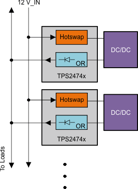 Figure 73. Block Diagram for Systems With Redundant DC/DC
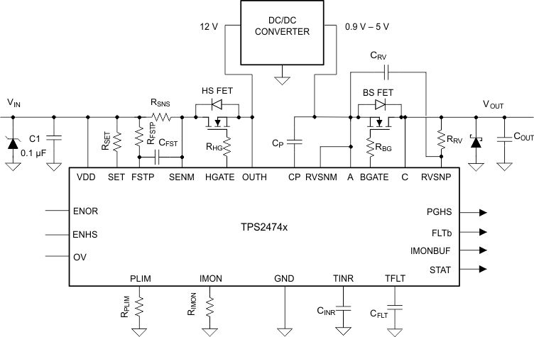 Figure 74. Application Schematic for Hot Swap, DC/DC, ORing Configuration