SLVSCV6A January 2015 – February 2015 TPS24740 , TPS24741 , TPS24742
PRODUCTION DATA.
- 1 Features
- 2 Applications
- 3 Description
- 4 Simplified Schematics
- 5 Revision History
- 6 Device Comparison Table
- 7 Pin Configuration and Functions
- 8 Specifications
-
9 Detailed Description
- 9.1 Overview
- 9.2 Functional Block Diagram
- 9.3
Feature Description
- 9.3.1 Internal Power ORing of TPS24740
- 9.3.2 Enable and Over-voltage Protection
- 9.3.3 Current Limit and Power Limit During Start-up
- 9.3.4 Two Level Protection During Regular Operation
- 9.3.5 Dual Timer (TFLT and TINR)
- 9.3.6 Using SoftStart - IHGATE and TINR Considerations
- 9.3.7 Three Options for Response to a Fast Trip
- 9.3.8 Programmable Reverse Voltage Threshold
- 9.3.9 Analog Current Monitor
- 9.3.10 Power Good Flag
- 9.3.11 ORing MOSFET Status Indicator
- 9.3.12 Fault Reporting
- 9.4 Device Functional Modes
-
10Application and Implementation
- 10.1 Application Information
- 10.2
Typical Application
- 10.2.1 30A Single channel OR then Hot Swap With Current Monitoring
- 10.2.2 Design Requirements
- 10.2.3
Detailed Design Procedure
- 10.2.3.1 Select RSNS and VSNS,CL Setting
- 10.2.3.2 Selecting the Fast Trip Threshold and Filtering
- 10.2.3.3 Selecting the Hot Swap FET(s)
- 10.2.3.4 Select Power Limit
- 10.2.3.5 Set Fault Timer
- 10.2.3.6 Check MOSFET SOA
- 10.2.3.7 Choose ORing MOSFET
- 10.2.3.8 Choose Reverse Current Threshold and Filtering
- 10.2.3.9 Choose Under Voltage and Over Voltage Settings
- 10.2.3.10 Selecting CIN, COUT, and CMIDDLE
- 10.2.3.11 Selecting D1 and D2
- 10.2.3.12 Ensuring Stability
- 10.2.3.13 Compute Tolerances
- 10.2.4 Application Curves
- 10.2.5
40 A Single Channel Hot Swap then ORing
- 10.2.5.1 Design Requirements
- 10.2.5.2
Design Procedure
- 10.2.5.2.1 Select RSNS and VSNS,CL Setting
- 10.2.5.2.2 Selecting the Fast Trip Threshold and Filtering
- 10.2.5.2.3 Selecting the Hot Swap FET
- 10.2.5.2.4 Select Power Limit
- 10.2.5.2.5 Set Fault Timer
- 10.2.5.2.6 Check MOSFET SOA
- 10.2.5.2.7 Checking Stability of Hot Swap Loop
- 10.2.5.2.8 Choose ORing MOSFET
- 10.2.5.2.9 Choose Reverse Current Threshold and Filtering
- 10.2.5.2.10 Choose Under Voltage and Over Voltage Settings
- 10.2.5.2.11 Selecting CIN, COUT, CMIDDLE, and Transient Protection
- 10.2.5.2.12 Adding CENHS
- 10.2.5.3 Application Curves
- 10.3 System Examples
- 11Power Supply Recommendations
- 12Layout
- 13Device and Documentation Support
- 14Mechanical, Packaging, and Orderable Information
Package Options
Mechanical Data (Package|Pins)
- RGE|24
Thermal pad, mechanical data (Package|Pins)
- RGE|24
Orderable Information
1 Features
- 2.5V to 18V Bus Operation (30V abs max)
- Programmable Protection Settings:
- Current Limit: ±5% at 10mV
- Fast Trip: ±10% at 20mV
- Reverse Voltage: ±1mV at –1 mV
- Programable Response Time for Fast Trip and Reverse Voltage
- Programmable FET SOA Protection
- Dual Timer (Inrush/Fault)
- Interchangeable Hot Swap and ORing
- Analog Current Monitor (1% at 25mV)
- Status Flags for Faults and Power Good
- UV and OV Protection
- Independent EN for Hot Swap and ORing
- 4mm × 4mm 24-pin QFN
- 40 = Latch, 41 = Retry, 42 = Fast Latch Off
2 Applications
- Enterprise Storage
- Power Muxing
- Redundant Power Supplies
- Battery Back Up
3 Description
The TPS2474x is an integrated ORing and Hot Swap controller for 2.5 V to 18 V systems. It's precise and programmable protection settings aid in the design of high power, high availability systems where isolating faults is critical.
Programmable current limit, fast shut down, and fault timer protect the load and supply during fault conditions such as a hot - short. The fast shutdown threshold and response time can be tuned to ensure a fast response to real faults, while avoiding nuisance trips. Programmable SOA (Safe Operating Area) protection and the inrush timer keep the MOSFET safe under all operating conditions. After asserting a power good, TPS2474x runs the fault timer during over-current events, but doesn't current limit. It shuts down after the fault timer expires. Two independent timers (inrush/fault) allow the user to customize protection based on system requirements. The ORing function of the TPS2474x allows the user to program the reverse voltage threshold and response time to aid in the design of redundant power supply systems.
Device Information(1)
| PART NUMBER | PACKAGE | BODY SIZE (NOM) |
|---|---|---|
| TPS24740 TPS24741 TPS24742 |
VQFN (24) | 4.00 mm x 4.00 mm |
- For all available packages, see the orderable addendum at the end of the data sheet.
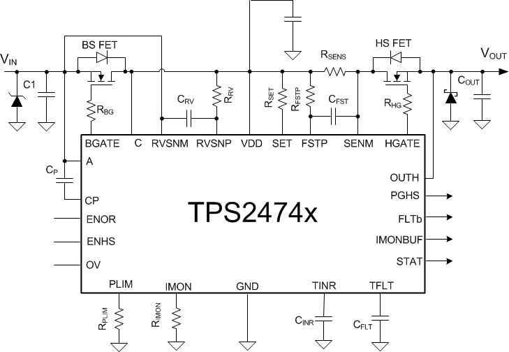
4 Simplified Schematics
 |
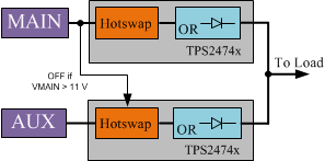
TPS2474x in Priority Muxing |
|