SLVSCV6A January 2015 – February 2015 TPS24740 , TPS24741 , TPS24742
PRODUCTION DATA.
- 1 Features
- 2 Applications
- 3 Description
- 4 Simplified Schematics
- 5 Revision History
- 6 Device Comparison Table
- 7 Pin Configuration and Functions
- 8 Specifications
-
9 Detailed Description
- 9.1 Overview
- 9.2 Functional Block Diagram
- 9.3
Feature Description
- 9.3.1 Internal Power ORing of TPS24740
- 9.3.2 Enable and Over-voltage Protection
- 9.3.3 Current Limit and Power Limit During Start-up
- 9.3.4 Two Level Protection During Regular Operation
- 9.3.5 Dual Timer (TFLT and TINR)
- 9.3.6 Using SoftStart - IHGATE and TINR Considerations
- 9.3.7 Three Options for Response to a Fast Trip
- 9.3.8 Programmable Reverse Voltage Threshold
- 9.3.9 Analog Current Monitor
- 9.3.10 Power Good Flag
- 9.3.11 ORing MOSFET Status Indicator
- 9.3.12 Fault Reporting
- 9.4 Device Functional Modes
-
10Application and Implementation
- 10.1 Application Information
- 10.2
Typical Application
- 10.2.1 30A Single channel OR then Hot Swap With Current Monitoring
- 10.2.2 Design Requirements
- 10.2.3
Detailed Design Procedure
- 10.2.3.1 Select RSNS and VSNS,CL Setting
- 10.2.3.2 Selecting the Fast Trip Threshold and Filtering
- 10.2.3.3 Selecting the Hot Swap FET(s)
- 10.2.3.4 Select Power Limit
- 10.2.3.5 Set Fault Timer
- 10.2.3.6 Check MOSFET SOA
- 10.2.3.7 Choose ORing MOSFET
- 10.2.3.8 Choose Reverse Current Threshold and Filtering
- 10.2.3.9 Choose Under Voltage and Over Voltage Settings
- 10.2.3.10 Selecting CIN, COUT, and CMIDDLE
- 10.2.3.11 Selecting D1 and D2
- 10.2.3.12 Ensuring Stability
- 10.2.3.13 Compute Tolerances
- 10.2.4 Application Curves
- 10.2.5
40 A Single Channel Hot Swap then ORing
- 10.2.5.1 Design Requirements
- 10.2.5.2
Design Procedure
- 10.2.5.2.1 Select RSNS and VSNS,CL Setting
- 10.2.5.2.2 Selecting the Fast Trip Threshold and Filtering
- 10.2.5.2.3 Selecting the Hot Swap FET
- 10.2.5.2.4 Select Power Limit
- 10.2.5.2.5 Set Fault Timer
- 10.2.5.2.6 Check MOSFET SOA
- 10.2.5.2.7 Checking Stability of Hot Swap Loop
- 10.2.5.2.8 Choose ORing MOSFET
- 10.2.5.2.9 Choose Reverse Current Threshold and Filtering
- 10.2.5.2.10 Choose Under Voltage and Over Voltage Settings
- 10.2.5.2.11 Selecting CIN, COUT, CMIDDLE, and Transient Protection
- 10.2.5.2.12 Adding CENHS
- 10.2.5.3 Application Curves
- 10.3 System Examples
- 11Power Supply Recommendations
- 12Layout
- 13Device and Documentation Support
- 14Mechanical, Packaging, and Orderable Information
Package Options
Mechanical Data (Package|Pins)
- RGE|24
Thermal pad, mechanical data (Package|Pins)
- RGE|24
Orderable Information
9 Detailed Description
9.1 Overview
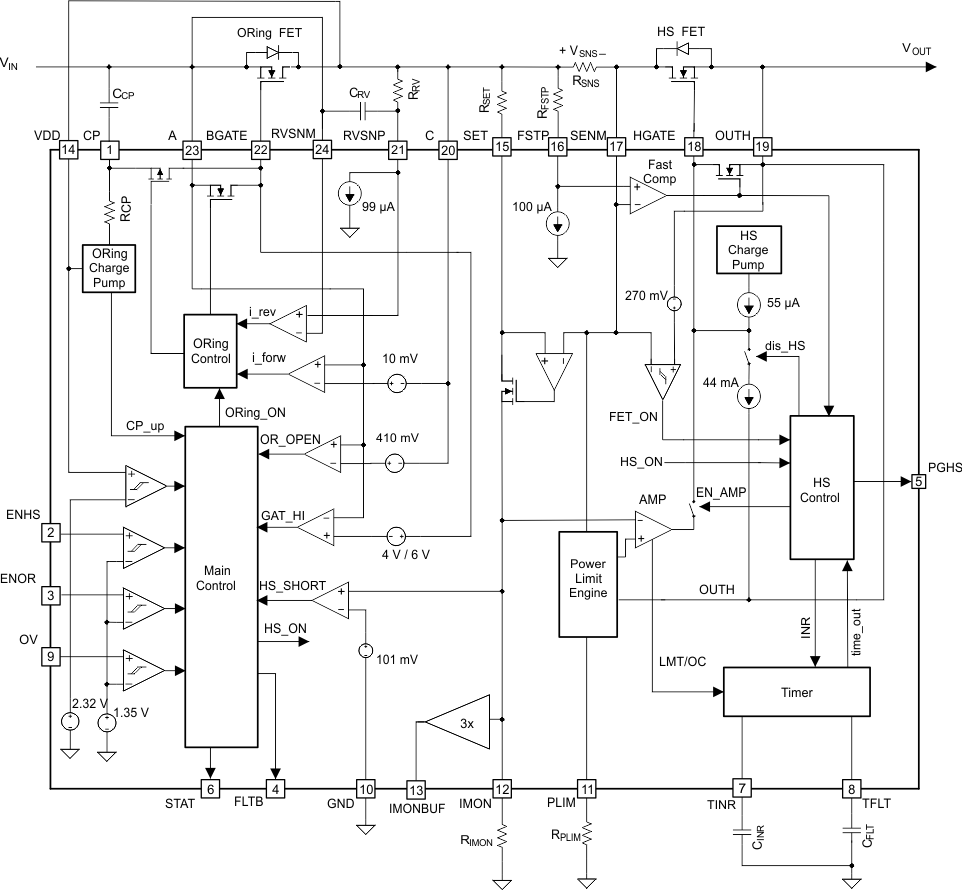
TPS2474x is a Hot Swap and ORing controller with many programmable settings. In addition the ORing and Hot Swap blocks are set-up independently, which allows for the interchangeable order of Hot Swap and ORing. For the ORing controller the RVSNM and RVSNP serve as a way to program the reverse voltage threshold and sense the reverse voltage. The Hot Swap features a programmable current limit, power limit, and fast trip threshold. It also has dual timers: one for inrush and one during over current faults. Finally it features an analog current monitor that can be used to provide current information to a microcontroller.
9.2 Functional Block Diagram
9.3 Feature Description
9.3.1 Internal Power ORing of TPS24740
The ORing function of the TPS2474x runs from an internal bus (VINT), which is derived from ORing A, C, and VDD. This ensures that the TPS2474x can stay powered and functions properly, even if the input or output are shorted to GND. The ORing function's UVLO is derived based on the VINT rail. This does mean that the part can draw up to 3 mA from the A or C pin. Hence it is recommended to keep traces to these pins fairly short and to avoid adding resistors in the path.
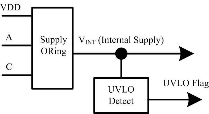 Figure 19. Power ORing
9.3.2 Enable and Over-voltage Protection
Both the Hot Swap section and the ORing section can be independently enabled with the ENHS and ENOR pins respectively. The part is enabled when the pin voltage exceeds 1.35V and is disabled when the pin voltage falls under 1.3V providing 50mV of hysteresis. A resistor divider can be connected to these pins to turn on the TSP2474x at a certain bus voltage. Both the ORing and the Hot Swap FETs will be turned off if the OV pin exceeds 1.35V.
9.3.3 Current Limit and Power Limit During Start-up
The current limit and power limit of the TPS2474x are programmable to protect the load, power supply, and the Hot Swap MOSFET. During start-up the active control loop will regulate the gate to ensure that the current through the MOSFET and the power dissipation of the MOSFET is below their respective pre-programmed thresholds. The maximum current allowed through the MOSFET (ILIM) is determined with Equation 1. ILIM,CL is the programmed current limit, PLIM is the programmed power limit, and VDS is the drain to source voltage across the Hot Swap MOSFET.

This results in an IV curve shown in Figure 20. ILIM,PL denotes the maximum allowed MOSFET current (IDS) when the part is in power limit. As VDS increases, ILIM,PL decreases and ILIM,PL,MIN denotes the lowest ILIM,PL, which occurs at the largest VDS (VDS,MAX). The TPS2474x enforce this by regulating the voltage across RSNS (VSNS). VSNS,PL denotes VSNS when power limiting is active. Similarly to ILIM,PL, VSNS,PL decreases as VDS increases and VSNS,PL,MIN corresponds to the lowest VSNS,PL, which occurs at VDS,MAX. VSNS,CL is a current limiting sense voltage, which is programmable in the TPS2474x.
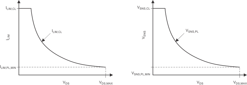 Figure 20. Current vs VDS and VSNS vs VDS Programmed by Power Limit Engine
The current and power limit can be programmed using the equations below.


Note, that the error is largest at VSNS,PL,MIN due to offset of the internal amplifier. Also the operation at VDS,MAX is most critical because it corresponds to the short circuit condition and has the biggest impact on start time. Thus it is critical to consider VSNS,PL,MIN during design. Equation 5 shows the relationship of VSNS,PL,MIN as a function of PLIM, ILIM,CL, VSNS,CL, and VDS,MAX. Note that ILIM,CL and VDS,MAX are usually determined by the system requirements. The designer will have control over PLIM and VSNS,CL. In general, there will be a desire to reduce the power limit to allow for smaller MOSFETs and to reduce the VSNS,CL to improve efficiency (lower RSNS). However, this will also reduce VSNS,PL,MIN and the designer should ensure that it's above the miminum recommended value of 1.5mV.

9.3.4 Two Level Protection During Regular Operation
After the TPS2474x has gone through start-up it will no longer actively control HGATE. Instead it will run the timer when the current is between the current limit and the fast trip threshold. Once the timer has expired the gate will be pulled down. If the current ever exceeds the fast trip threshold, HGATE will be pulled down immediately.
9.3.5 Dual Timer (TFLT and TINR)
TPS2474x has two timer pins to allow the user to customize the protection. The TINR pin sources 10.25 µA when the device is in start-up mode and is actively regulating the gate to limit the MOSFET power or current. It sinks 2 µA otherwise. The TFLT pin sources 10.25 µA when the device is in regular operation and the FET current exceeds the current limit. It sinks 2 µA otherwise. If either of the timer pins exceeds 1.35, the TPS2474x times out. The TPS24740 and TPS24742 latches off. The TPS24741 goes through 64 cycles of TINR and attempts to start-up again.
Since the TINR usually runs when the MOSFET is being stressed, TINR should be sized to maintain the FET within its SOA. In general TFLT runs when the load is drawing more current than expected, which can stress the load and the power supply. Thus TFLT should be programmed to have the right protection settings for the power supply and the load. In some systems the load is allowed to draw current above the current limit for a prolonged time. In that case a large TFLT is required, but a short TINR may still be desired to minimize the worst case FET stress. In other applications a long TINR may be required to due to large downstream capacitances, but drawing excessive current from the power supply for more than 5ms is not desired. In that case a short TFLT and a long TINR should be used. Finally, many applications can use the same TINR and TFLT setting, in which case the pins can be tied together and a single capacitor can be used. The two different options are shown in Figure 21.
 Figure 21. Timer Configurations
If two separate timer capacitors are used their values can be computed with Equation 6 and Equation 7:
If a single capacitor is used CTMR can be computed with Equation 8.
9.3.6 Using SoftStart – IHGATE and TINR Considerations
During start-up the TPS2474x regulates the HGATE to keep the FET power dissipation within PLIM. This is accomplished by an amplifier that monitors the IMON voltage and an internal reference voltage. The TPS24740 will source current into HGATE if VIMON is lower than the reference voltage and will sink current into HGATE if VIMON is above the reference voltage. In steady state, the VIMON will be regulated to the VIMON,PL point, where IHGATE equals zero. Note that VIMON,PL is determined by RPLIM and the VSENM – VOUTH.
The same amplifier feeds into the inrush timer circuitry to run the timer when the part is in power limit. The VIMON threshold at which the timer starts to source current is denoted as VIMON, TINR. Note that VIMON,TINR is lower than VIMON,PL to account for tolerances and ensure that the timer is always active when the device is in power limit. The difference between the two thresholds is defined as ΔVIMON, TINR. A typical curve of the IHGATE and ITINR is available in the typical characteristics section.
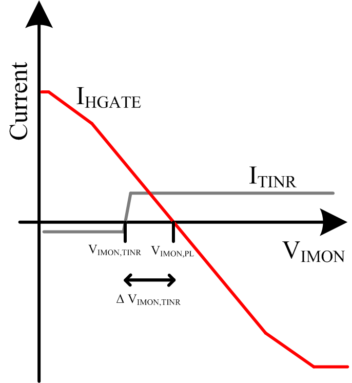 Figure 22. IHGATE Current and TINR Relationship
It is critical to consider ΔVIMON, TINR and Figure 22 if a soft start circuit is used. Typically, the soft start is implemented by limiting the gate dv/dt with a capacitor, which in turn limits the inrush current to the output capacitor. Often times, the inrush current is kept below ILIM,PL to keep the timer from running. Note that the ILIM,PL is based on the VIMON,PL threshold and thus TINR can be activated even if the inrush current is below ILIM,PL. To prevent the timer from running unintentionally, it's important that the minimum power limit (typical PLIM - tolerance) is above PLIM,MIN,SS, which can be computed as shown in Equation 9 below. As an example, consider the usage case where the maximum inrush current (IINR,MAX) is 2A, the maximum input voltage (VIN,MAX) is 13V and RSET, RIMON, and RSNS are 100Ω, 2.7kΩ, and 1mΩ respectively. For that case the power limit should be set to at least 58.3 W + PLIM tolerance to ensure that the inrush timer does not run.

9.3.7 Three Options for Response to a Fast Trip
The TPS24740, TPS24741, and TPS24742 have difference responses to a fast trip event to accommodate different design requirements. When the current exceeds the fast trip threshold, the gate is quickly pulled down to minimize damage that can be caused due to a short circuit. Figure 23 shows the response of the variate devices options to a Hotshort on the output. The TPS24740 (latch) attempts to re-start once after the hot-short is observed and then stay off. The TPS24741 continuously retries with a duty cycle of ~0.5% (0.7% if TFLT and TINR are connected, 0.35% if TFLT and TINR are not connected); and, the TPS24742 shuts off and never retries again. In general the TPS24742 (Fast/immediate Latch Off) places the least amount of stress on the MOSFET, but is the least likely to recover from a nuisance trip.
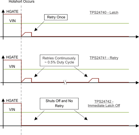 Figure 23. TPS24740/1/2 Response to a Short Circuit
9.3.8 Programmable Reverse Voltage Threshold
The TPS2474x has a programmable reverse voltage threshold. An internal comparator detects a reverse current condition when RVSNP is above RVSNM. This signal is used to shut off the ORing MOSFET. RRV along with a 99µA current source pre-bias RVSNP to below the real source voltage of the MOSFET and effectively set the reverse voltage threshold. CRV along with RRV filters transients across the drain to source of the ORing FET.
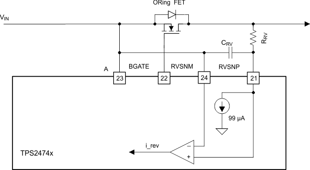 Figure 24. Programming and Sensing Reverse Voltage
Note that the RVSNM and RVSNP can be connected at various places. One option is to connect it across the drain to source of the ORing FET (Figure 24), which would result in a reverse current threshold of VRV/RDSON. Another option is to connect across the RSNS as shown in Figure 25. This could be useful if a precise threshold is desired and RSNS is larger than the RDSON of the ORing FET.
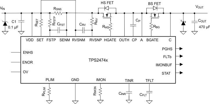 Figure 25. Sensing Reverse Voltage Across Hot Swap Sense Resistor
9.3.9 Analog Current Monitor
The TPS2474x also features two analog current monitoring outputs: IMON and IMONBUF. Each has their own advantages and disadvantages. The IMON is more accurate, because it doesn’t have the error added from the second stage. However it is a high impedance output and leakage current on that node would result in monitoring error. In addition it can only support 30pF of capacitance and its full scale range is 675mV (this is where current limit kicks in). The IMONBUF takes the IMON signal and buffers it 3x. This introduces more error, but the output is low impedance, has a larger full scale range, and can drive up to 100pF of capacitance.
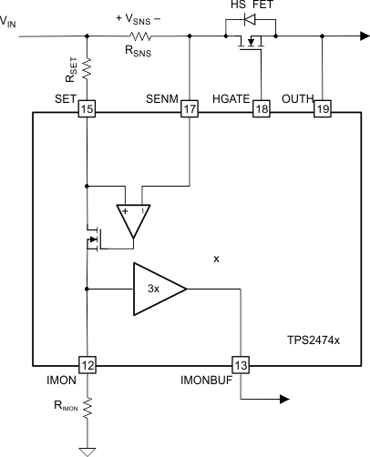 Figure 26. Current Monitoring Circuitry
9.3.10 Power Good Flag
The TPS2474x has a power good flag, which should be used to turn on downstream DC/DC converters. This reduces the stress on the Hot Swap MOSFET during start-up. The PGHS pin of the TPS2474x is asserted (with 1 ms deglitch) when both:
- Hot Swap is enabled and
- VDS of Hot Swap MOSFET is below 240 mV.
PGHS is de-asserted (with 8 ms deglitch) when either:
- Hot Swap is disabled.
- VDS of Hot Swap MOSFET is above 310 mV
- In an overcurrent condition that causes the timer to time out and latch off.
9.3.11 ORing MOSFET Status Indicator
The TPS2474x, features a STAT flag that indicates whether the BGATE (ORing FET driver) is ON or OFF. In general it is good practice to have the ORing FETs ON before drawing any significant load to prevent the ORing FET from overheating.
9.3.12 Fault Reporting
TPS 2474x will assert a fault by pulling down on the FLTb pin if any of the following occur:
- Hot Swap MOSFET Shorted Fault ( ENHS = LO, but VIMON > 101 mV)
- Hot Swap timer times out.
- ORing MOSFET Open Fault (ENOR = HI, CP up, but VAC > 410 mV)
- CP is down for more than 32 ms
- Over Temperature Shut Down (OTSD)
Figure 27 shows the logic for the fault conditions.
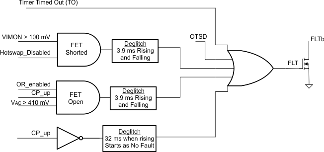 Figure 27. Logic for Fault Reporting
9.4 Device Functional Modes
The Hot Swap and ORing section of the TPS2474x are for the most part independent. The only exception is that the Hot Swap is gated by the charge pump being up. This ensures that the ORing FET is ON before the Hot Swap turns on to avoid a possible glitch from a fast ORing turn on.
9.4.1 ORing Functional Modes
Figure 28 shows the state machine for the ORing portion of the controller. It has three modes listed below:
- Precharge CP: Here the TPS2474x charges the CP node before beginning regular operation. This state is entered after POR/UVLO or if the CP voltage falls below 3.7V. Whenever the CP voltage is above 5.5V the FET OFF state is entered
- FET OFF: In this state the ORing FET is OFF and is pulled down to A with a 35mA current source. If a forward voltage drop is detected across the FET (VAC > 10mV) the TPS2474x enters the FET ON state. There is a 30mA fast pull up that lasts 20µs, followed by a sustained 0.3 mA pull up.
- FET ON: In this state the ORing FET is pulled up to the CP voltage. If reverse current is detected (RVSNP > RVSNM) the TPS2474x will enter the OFF state. There is a 0.9A pull down current that lasts 15 µs, followed by a sustained 35mA pull down.
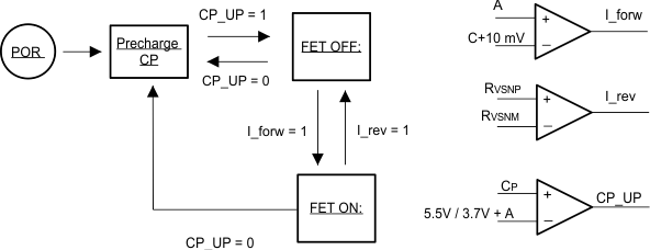 Figure 28. ORing State Machine
9.4.2 Hot Swap Functional Modes
The state machine for the Hot Swap section is shown in Figure 29. After a POR / UVLO event the Hot Swap waits 1.9ms after the charge pump is up before starting up. Once operational the Hot Swap has the following functional modes:
- Inrush Mode (INR): In this state the Hot Swap controller is actively regulating the HGATE to meet the current limit and power limit settings. The inrush timer is running if the controller is in power or current limiting. If the inrush timer times out the gate will be pulled down. The TPS24740 and TPS24742 will go to latched mode and TPS24741 will go into retry mode.
- Regular Operation Mode (REG): In this mode everything is operating properly so both the timers are discharged and the HGATE is high. If there is an overcurrent condition (VSNS > VSNS,CL), the device will go into fault mode. If there is a fast trip condition (VSNS > VFSTP), the gate will be pulled down with a 1A / 63 µs pulse. The TPS24742 will go to the latched state and the TPS24740 and TPS24741 will go back to inrush for a retry.
- Fault Mode (FLT): In this mode the TPS2474x runs the fault timer. Once the timer expires the TPS24740 and TPS24742 will go to latch mode while TPS24741 will go to retry mode. If the overcurrent condition is removed the controller will go back to the regular operation mode.
- Latched Mode (Latched): In the latched mode the HGATE is low, the timer is being discharged, and the FLTb is asserted. If there is a rising edge on ENHS the part will discharge the timers and go to the inrush mode.
- Retry Mode (Retry): Here the part charges and discharges the inrush timer 64 times before attempting another retry.
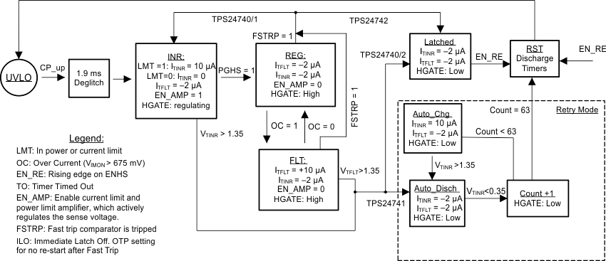 Figure 29. Hot Swap State Machine