SLVSE11A May 2017 – May 2017 TPS2547
PRODUCTION DATA.
- 1 Features
- 2 Applications
- 3 Description
- 4 Revision History
- 5 Pin Configuration and Functions
- 6 Specifications
- 7 Parameter Measurement Information
-
8 Detailed Description
- 8.1 Overview
- 8.2 Functional Block Diagram
- 8.3
Feature Description
- 8.3.1 Standard Downstream Port (SDP) USB 2.0/USB 3.0
- 8.3.2 Charging Downstream Port (CDP)
- 8.3.3 Dedicated Charging Port (DCP)
- 8.3.4 Wake on USB Feature (Mouse/Keyboard Wake Feature)
- 8.3.5 Load Detect
- 8.3.6 Power Wake
- 8.3.7 Port Power Management (PPM)
- 8.3.8 Overcurrent Protection
- 8.3.9 FAULT Response
- 8.3.10 Undervoltage Lockout (UVLO)
- 8.3.11 Thermal Sense
- 8.4 Device Functional Modes
- 9 Application and Implementation
- 10Power Supply Recommendations
- 11Layout
- 12Device and Documentation Support
- 13Mechanical, Packaging, and Orderable Information
Package Options
Mechanical Data (Package|Pins)
- RTE|16
Thermal pad, mechanical data (Package|Pins)
- RTE|16
Orderable Information
6 Specifications
6.1 Absolute Maximum Ratings
Over operating free-air temperature range (unless otherwise noted)(1)| MIN | MAX | UNIT | ||
|---|---|---|---|---|
| Voltage | IN, EN, ILIM_LO, ILIM_HI, FAULT, STATUS, ILIM_SEL, CTL1, CTL2, CTL3, OUT | –0.3 | 7 | V |
| IN to OUT | –7 | 7 | ||
| DP_IN, DM_IN, DP_OUT, DM_OUT | –0.3 | (IN + 0.3) or 5.7 | ||
| Input clamp current | DP_IN, DM_IN, DP_OUT, DM_OUT | ±20 | mA | |
| Continuous current in SDP or CDP mode | DP_IN to DP_OUT or DM_IN to DM_OUT | ±100 | mA | |
| Continuous current in BC1.2 DCP mode | DP_IN to DM_IN | ±50 | mA | |
| Continuous output current | OUT | Internally limited | ||
| Continuous output sink current | FAULT, STATUS | 25 | mA | |
| Continuous output source current | ILIM_LO, ILIM_HI | Internally limited | mA | |
| Operating junction temperature, TJ | –40 | Internally limited | °C | |
(1) Stresses beyond those listed under Absolute Maximum Ratings may cause permanent damage to the device. These are stress ratings only, which do not imply functional operation of the device at these or any other conditions beyond those indicated under Recommended Operating Conditions. Exposure to absolute-maximum-rated conditions for extended periods may affect device reliability.
6.2 ESD Ratings
| VALUE | UNIT | ||||
|---|---|---|---|---|---|
| V(ESD) | Electrostatic discharge | Human-body model (HBM), per ANSI/ESDA/JEDEC JS-001(1) | HBM | ±2000 | V |
| HBM wrt GND and each other, DP_IN, DM_IN, OUT | ±8000 | ||||
| Charged-device model (CDM), per JEDEC specification JESD22-C101(2) | ±500 | ||||
(1) JEDEC document JEP155 states that 500-V HBM allows safe manufacturing with a standard ESD control process.
(2) JEDEC document JEP157 states that 250-V CDM allows safe manufacturing with a standard ESD control process.
6.3 Recommended Operating Conditions
voltages are referenced to GND (unless otherwise noted)| MIN | MAX | UNIT | |||
|---|---|---|---|---|---|
| VIN | Input voltage, IN | 4.5 | 5.5 | V | |
| Input voltage, logic-level inputs, EN, CTL1, CTL2, CTL3, ILIM_SEL | 0 | 5.5 | V | ||
| Input voltage, data line inputs, DP_IN, DM_IN, DP_OUT, DM_OUT | 0 | VIN | V | ||
| VIH | High-level input voltage, EN, CTL1, CTL2, CTL3, ILIM_SEL | 1.8 | V | ||
| VIL | Low-level input voltage, EN, CTL1, CTL2, CTL3, ILIM_SEL | 0.8 | V | ||
| Continuous current, data line inputs, SDP or CDP mode, DP_IN to DP_OUT, DM_IN to DM_OUT | ±30 | mA | |||
| Continuous current, data line inputs, BC1.2 DCP mode, DP_IN to DM_IN | ±15 | mA | |||
| IOUT | Continuous output current, OUT | TJ = –40°C to 125°C | 0 | 2.5 | A |
| TJ = –40°C to 115°C | 0 | 3.0 | |||
| Continuous output sink current, FAULT, STATUS | 0 | 10 | mA | ||
| RILIM_XX | Current-limit set resistors | 15.4 | 750 | kΩ | |
| TJ | Operating virtual junction temperature | –40 | 125 | °C | |
6.4 Thermal Information
| THERMAL METRIC(1) | TPS2547 | UNIT | |
|---|---|---|---|
| RTE (WQFN) | |||
| 16 PINS | |||
| RθJA | Junction-to-ambient thermal resistance | 53.4 | °C/W |
| RθJC(top) | Junction-to-case (top) thermal resistance | 51.4 | °C/W |
| RθJB | Junction-to-board thermal resistance | 17.2 | °C/W |
| ψJT | Junction-to-top characterization parameter | 3.7 | °C/W |
| ψJB | Junction-to-board characterization parameter | 20.7 | °C/W |
| RθJC(bot) | Junction-to-case (bottom) thermal resistance | 3.9 | °C/W |
(1) For more information about traditional and new thermal metrics, see the Semiconductor and IC Package Thermal Metrics application report.
6.5 Electrical Characteristics
Unless otherwise noted: –40 ≤ TJ ≤ 125°C, 4.5 V ≤ VIN ≤ 5.5 V, VEN = VIN, VILIM_SEL = VIN, VCTL1 = VCTL2 = VCTL3 = VIN. RFAULT = RSTATUS = 10 kΩ, RILIM_HI = 20 kΩ, RILIM_LO = 80.6 kΩ. Positive currents are into pins. Typical values are at 25°C. All voltages are with respect to GND.| PARAMETER | TEST CONDITIONS | MIN | TYP | MAX | UNIT | |
|---|---|---|---|---|---|---|
| POWER SWITCH | ||||||
| RDS(on) | ON resistance(1) | TJ = 25°C, IOUT = 2 A | 73 | 84 | mΩ | |
| –40°C ≤ TJ ≤ 85°C, IOUT = 2 A | 73 | 105 | ||||
| –40°C ≤ TJ ≤ 125°C, IOUT = 2 A | 73 | 120 | ||||
| tr | OUT voltage rise time | VIN = 5 V, CL = 1 µF, RL = 100 Ω (see Figure 23 and Figure 24) | 0.7 | 1 | 1.6 | ms |
| tf | OUT voltage fall time | 0.2 | 0.35 | 0.5 | ||
| ton | OUT voltage turnon time | VIN = 5 V, CL = 1 µF, RL = 100 Ω (see Figure 23 and Figure 25) | 2.7 | 4 | ms | |
| toff | OUT voltage turnoff time | 1.7 | 3 | |||
| IREV | Reverse leakage current | VOUT = 5.5 V, VIN = VEN = 0 V, –40 ≤ TJ ≤ 85°C, Measure IOUT |
2 | µA | ||
| DISCHARGE | ||||||
| RDCHG | OUT discharge resistance | 400 | 500 | 630 | Ω | |
| tDCHG_L | Long OUT discharge hold time | Time VOUT < 0.7 V (see Figure 26) | 1.3 | 2 | 2.9 | s |
| tDCHG_S | Short OUT discharge hold time | Time VOUT < 0.7 V (see Figure 26) | 205 | 310 | 450 | ms |
| EN, ILIMSEL, CTL1, CTL2, CTL3 INPUTS | ||||||
| Input pin rising logic threshold voltage | 1 | 1.35 | 1.7 | V | ||
| Input pin falling logic threshold voltage | 0.85 | 1.15 | 1.45 | |||
| Hysteresis(2) | 200 | mV | ||||
| Input current | Pin voltage = 0 V or 5.5 V | –0.5 | 0.5 | µA | ||
| ILIMSEL CURRENT LIMIT | ||||||
| IOS | OUT short-circuit current limit(1) | VILIM_SEL = 0 V, RILIM_LO = 210 kΩ | 213 | 250 | 287 | mA |
| VILIM_SEL = 0 V, RILIM_LO = 80.6 kΩ | 598 | 650 | 708 | |||
| VILIM_SEL = 0 V, RILIM_LO = 22.1 kΩ | 2200 | 2365 | 2530 | |||
| VILIM_SEL = VIN, RILIM_HI= 20 kΩ | 2425 | 2610 | 2800 | |||
| VILIM_SEL = VIN, RILIM_HI = 16.9 kΩ | 2875 | 3085 | 3300 | |||
| VILIM_SEL = VIN, RILIM_HI = 15.4 kΩ, TJ = –40°C to 115°C | 3150 | 3375 | 3600 | |||
| tIOS | Response time to OUT short-circuit(2) | VIN = 5 V, R = 0.1Ω, lead length = 2 inches (see Figure 27) |
1.5 | µs | ||
| SUPPLY CURRENT | ||||||
| IIN_OFF | Disabled IN supply current | VEN = 0 V, VOUT = 0 V, –40 ≤ TJ ≤ 85°C | 0.1 | 2 | µA | |
| IIN_ON | Enabled IN supply current | VCTL1 = VCTL2 = VIN, VCTL3 = 0 V, VILIM_SEL = 0 V | 165 | 220 | µA | |
| VCTL1 = VCTL2 = VCTL3 = VIN, VILIM_SEL = 0 V | 175 | 230 | ||||
| VCTL1 = VCTL2 = VIN, VCTL3 = 0 V, VILIM_SEL = VIN | 185 | 240 | ||||
| VCTL1 = VCTL2 = VIN, VCTL3 = VIN, VILIM_SEL = VIN | 195 | 250 | ||||
| VCTL1 = 0 V, VCTL2 = VCTL3 = VIN | 215 | 270 | ||||
| UNDERVOLTAGE LOCKOUT | ||||||
| VUVLO | IN rising UVLO threshold voltage | 3.9 | 4.1 | 4.3 | V | |
| Hysteresis(2) | 100 | mV | ||||
| FAULT | ||||||
| Output low voltage | IFAULT = 1 mA | 100 | mV | |||
| OFF-state leakage | VFAULT = 5.5 V | 1 | µA | |||
| Overcurrent FAULT rising and falling deglitch | 5 | 8.2 | 12 | ms | ||
| STATUS | ||||||
| Output low voltage | ISTATUS = 1 mA | 100 | mV | |||
| OFF-state leakage | VSTATUS = 5.5 V | 1 | µA | |||
| THERMAL SHUTDOWN | ||||||
| Thermal shutdown threshold | 155 | °C | ||||
| Thermal shutdown threshold in current-limit | 135 | |||||
| Hysteresis(2) | 20 | |||||
(1) Pulse-testing techniques maintain junction temperature close to ambient temperature; Thermal effects must be taken into account separately.
(2) These parameters are provided for reference only and do not constitute part of TI's published device specifications for purposes of TI's product warranty.
6.6 Electrical Characteristics: High-Bandwidth Switch
Unless otherwise noted: –40 ≤ TJ ≤ 125°C, 4.5 V ≤ VIN ≤ 5.5 V, VEN = VIN, VILIM_SEL = VIN, VCTL1 = VCTL2 = VCTL3 = VIN. RFAULT = RSTATUS = 10 kΩ, RILIM_HI = 20 kΩ, RILIM_LO = 80.6 kΩ. Positive currents are into pins. Typical values are at 25°C. All voltages are with respect to GND.| PARAMETER | TEST CONDITIONS | MIN | TYP | MAX | UNIT | |
|---|---|---|---|---|---|---|
| HIGH-BANDWIDTH ANALOG SWITCH | ||||||
| DP/DM switch ON resistance | VDP/DM_OUT = 0 V, IDP/DM_IN = 30 mA | 2 | 4 | Ω | ||
| VDP/DM_OUT = 2.4 V, IDP/DM_IN = –15 mA | 3 | 6 | ||||
| Switch resistance mismatch between DP / DM channels |
VDP/DM_OUT = 0 V, IDP/DM_IN = 30 mA | 0.05 | 0.15 | Ω | ||
| VDP/DM_OUT = 2.4 V, IDP/DM_IN = –15 mA | 0.05 | 0.15 | ||||
| DP/DM switch OFF-state capacitance(1) | VEN= 0 V, VDP/DM_IN = 0.3 V, Vac = 0.6 Vpk–pk, f = 1 MHz |
3 | 3.6 | pF | ||
| DP/DM switch ON-state capacitance(2) | VDP/DM_IN = 0.3 V, Vac = 0.6 Vpk-pk, f = 1 MHz | 5.4 | 6.2 | pF | ||
| OIRR | OFF-state isolation(3) | VEN= 0 V, f = 250 MHz | 33 | dB | ||
| XTALK | ON-state cross channel isolation(3) | f = 250 MHz | 52 | dB | ||
| OFF-state leakage current | VEN = 0 V, VDP/DM_IN = 3.6 V, VDP/DM_OUT = 0 V, measure IDP/DM_OUT | 0.1 | 1.5 | µA | ||
| BW | Bandwidth (–3 dB)(3) | RL = 50 Ω | 2.6 | GHz | ||
| tpd | Propagation delay(3) | 0.25 | ns | |||
| tSK | Skew between opposite transitions of the same port (tPHL – tPLH) | 0.1 | 0.2 | ns | ||
(1) The resistance in series with the parasitic capacitance to GND is typically 250 Ω.
(2) The resistance in series with the parasitic capacitance to GND is typically 150 Ω
(3) These parameters are provided for reference only and do not constitute part of TI's published device specifications for purposes of TI's product warranty.
6.7 Electrical Characteristics: Charging Controller
Unless otherwise noted: –40 ≤ TJ ≤ 125°C, 4.5 V ≤ VIN ≤ 5.5 V, VEN = VIN, VILIM_SEL = VIN, VCTL1 = 0 V, VCTL2 = VCTL3 = VIN. RFAULT = RSTATUS = 10 kΩ, RILIM_HI = 20 kΩ, RILIM_LO = 80.6 kΩ. Positive currents are into pins. Typical values are at 25°C. All voltages are with respect to GND.| PARAMETER | TEST CONDITIONS | MIN | TYP | MAX | UNIT | ||
|---|---|---|---|---|---|---|---|
| SHORTED MODE (BC1.2 DCP) | |||||||
| DP_IN / DM_IN shorting resistance | VCTL1 = VIN, VCTL2 = VCTL3 = 0 V | 125 | 200 | Ω | |||
| 1.2 V MODE | |||||||
| DP_IN /DM_IN output voltage | VCTL1 = VIN, VCTL2 = VCTL3 = 0 V | 1.19 | 1.25 | 1.31 | V | ||
| DP_IN /DM_IN output impedance | 60 | 75 | 94 | kΩ | |||
| DIVIDER1 MODE | |||||||
| DP_IN divider1 output voltage | VCTL1 = VIN, VCTL2 = VCTL3 = 0 V | 1.9 | 2 | 2.1 | V | ||
| DM_IN divider1 output voltage | 2.57 | 2.7 | 2.84 | V | |||
| DP_IN output impedance | 8 | 10.5 | 12.5 | kΩ | |||
| DM_IN output impedance | 8 | 10.5 | 12.5 | kΩ | |||
| DIVIDER2 MODE | |||||||
| DP_IN divider2 output voltage | IOUT = 1 A | 2.57 | 2.7 | 2.84 | V | ||
| DM_IN divider2 output voltage | 1.9 | 2 | 2.1 | V | |||
| DP_IN output impedance | 8 | 10.5 | 12.5 | kΩ | |||
| DM_IN output impedance | 8 | 10.5 | 12.5 | kΩ | |||
| CHARGING DOWNSTREAM PORT | |||||||
| VDM_SRC | DM_IN CDP output voltage | VCTL1 = VCTL2 = VCTL3 = VIN | VDP_IN = 0.6 V, –250 µA < IDM_IN < 0 µA |
0.5 | 0.6 | 0.7 | V |
| VDAT_REF | DP_IN rising lower window threshold for VDM_SRC activation | VCTL1 = VCTL2 = VCTL3 = VIN | 0.25 | 0.4 | V | ||
| Hysteresis(1) | 50 | mV | |||||
| VLGC_SRC | DP_IN rising upper window threshold for VDM_SRC de-activation | 0.8 | 1 | V | |||
| Hysteresis(1) | 100 | mV | |||||
| IDP_SINK | DP_IN sink current | VCTL1 = VCTL2 = VCTL3 = VIN | VDP_IN = 0.6 V | 40 | 70 | 100 | µA |
| LOAD DETECT – NON-POWER WAKE | |||||||
| ILD | IOUT rising load detect current threshold | VCTL1 = VCTL2 = VCTL3 = VIN | 635 | 700 | 765 | mA | |
| Hysteresis(1) | 50 | mA | |||||
| tLD_SET | Load detect set time | 140 | 200 | 275 | ms | ||
| Load detect reset time | 1.9 | 3 | 4.2 | s | |||
| LOAD DETECT – POWER WAKE | |||||||
| IOS_PW | Power wake short-circuit current limit | VCTL1 = VCTL2 = 0 V, VCTL3 = VIN | 32 | 55 | 78 | mA | |
| IOUT falling power wake reset current detection threshold | 23 | 45 | 67 | mA | |||
| Reset current hysteresis(1) | 5 | mA | |||||
| Power wake reset time | 10.7 | 15 | 20.6 | s | |||
(1) These parameters are provided for reference only and do not constitute part of Texas Instrument's published device specifications for purposes of Texas Instrument's product warranty.
6.8 Typical Characteristics
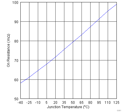 Figure 1. Power Switch ON Resistance vs Temperature
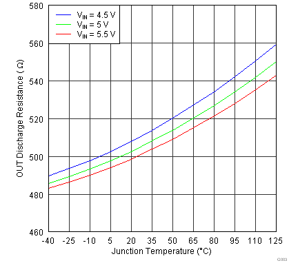 Figure 3. OUT Discharge Resistance vs Temperature
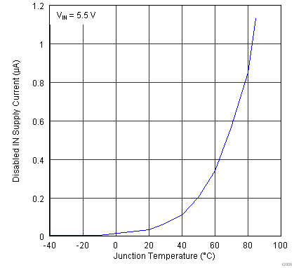 Figure 5. Disabled in Supply Current vs Temperature
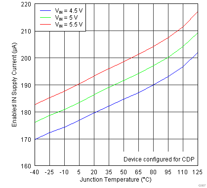 Figure 7. Enabled in Supply Current - CDP vs Temperature
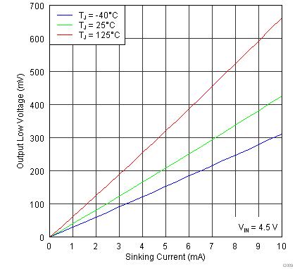 Figure 9. Status and Fault Output Low Voltage
vs Sinking Current
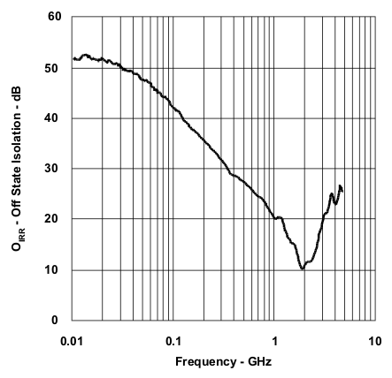 Figure 11. OFF-State Data Switch Isolation vs Frequency
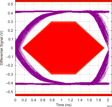 Figure 13. Eye Diagram Using USB Compliance Test Pattern (With No Switch)
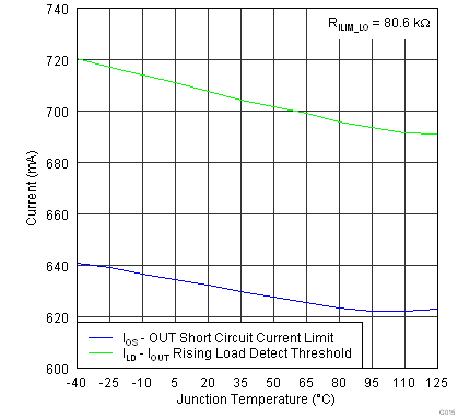 Figure 15. IOUT Rising Load Detect Threshold and Out Short-Circuit Current Limit vs Temperature
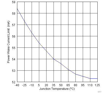 Figure 17. Power Wake Current Limit vs Temperature
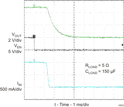 Figure 19. Turnoff Response
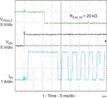 Figure 21. Device Enabled Into Short-Circuit - Thermal Cycling
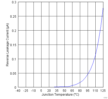 Figure 2. Reverse Leakage Current vs Temperature
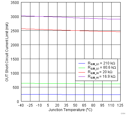 Figure 4. OUT Short-Circuit Current Limit vs Temperature
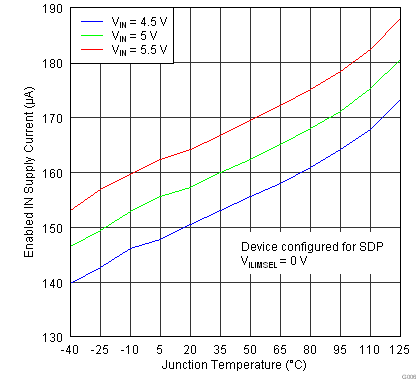 Figure 6. Enabled in Supply Current - SDP vs Temperature
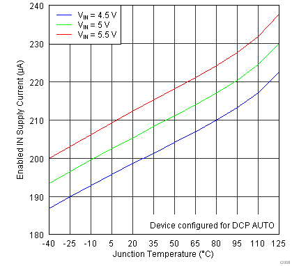 Figure 8. Enabled in Supply Current - DCP Auto
vs Temperature
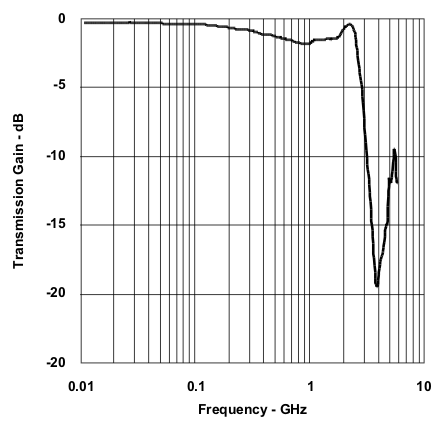 Figure 10. Data Transmission Characteristics vs Frequency
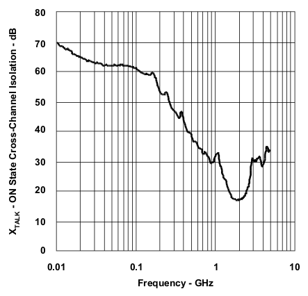 Figure 12. ON-State Cross-Channel Isolation vs Frequency
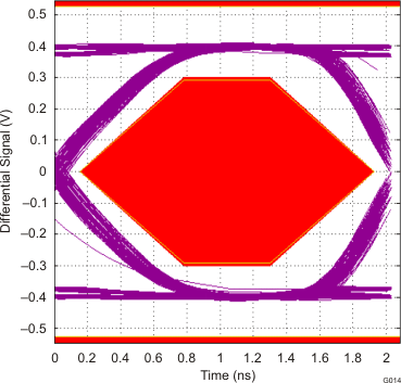 Figure 14. Eye Diagram Using USB Compliance Test Pattern (With Data Switch)
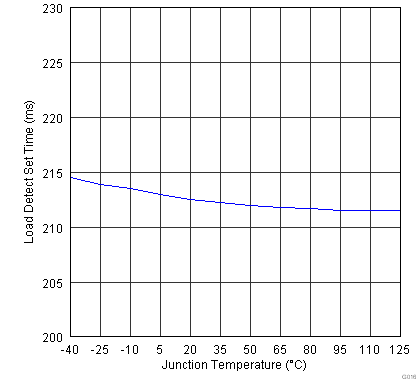 Figure 16. Load Detect Set Time vs Temperature
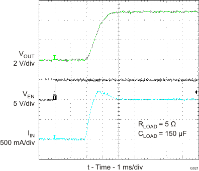 Figure 18. Turnon Response
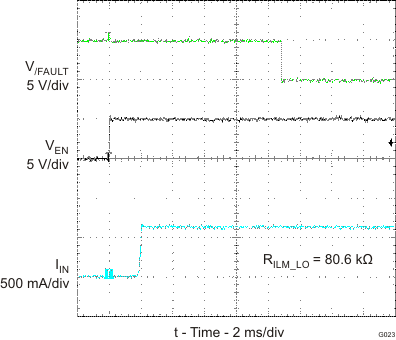 Figure 20. Device Enabled Into Short-Circuit
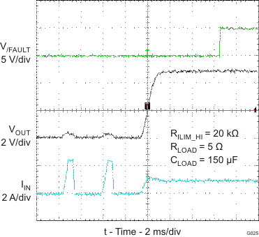 Figure 22. Short-Circuit to Full Load Recovery