SLVSGP9 October 2023 TPS25730
PRODUCTION DATA
- 1
- 1 Features
- 2 Applications
- 3 Description
- 4 Device Comparison Table
- 5 Pin Configuration and Functions
-
6 Specifications
- 6.1 Absolute Maximum Ratings
- 6.2 ESD Ratings
- 6.3 Recommended Operating Conditions
- 6.4 Recommended Capacitance
- 6.5 Thermal Information
- 6.6 Power Supply Characteristics
- 6.7 Power Consumption
- 6.8 PPHV Power Switch Characteristics - TPS25730D
- 6.9 PP_EXT Power Switch Characteristics - TPS25730S
- 6.10 Power Path Supervisory
- 6.11 CC Cable Detection Parameters
- 6.12 CC PHY Parameters
- 6.13 Thermal Shutdown Characteristics
- 6.14 ADC Characteristics
- 6.15 Input/Output (I/O) Characteristics
- 6.16 I2C Requirements and Characteristics
- 6.17 Typical Characteristics
- 7 Parameter Measurement Information
-
8 Detailed Description
- 8.1 Overview
- 8.2 Functional Block Diagram
- 8.3
Feature Description
- 8.3.1 USB-PD Physical Layer
- 8.3.2 Power Management
- 8.3.3 Power Paths
- 8.3.4 Cable Plug and Orientation Detection
- 8.3.5 Overvoltage Protection (CC1, CC2)
- 8.3.6 Default Behavior Configuration (ADCIN1, ADCIN2)
- 8.3.7 ADC
- 8.3.8 Digital Interfaces
- 8.3.9 Digital Core
- 8.3.10 I2C Interface
- 8.3.11 Minimum Voltage Configuration
- 8.3.12 Maximum Voltage Configuration
- 8.3.13 Sink Current Configuration
- 8.3.14 Autonegotiate Sink Minimum Power
- 8.3.15 Extended Sink Capabilities Power Delivery Power
- 8.4 Device Functional Modes
- 8.5 Schottky for Current Surge Protection
- 8.6 Thermal Shutdown
- 9 Application and Implementation
- 10Device and Documentation Support
- 11Revision History
- 12Mechanical, Packaging, and Orderable Information
Package Options
Mechanical Data (Package|Pins)
Thermal pad, mechanical data (Package|Pins)
- RSM|32
Orderable Information
8.3.1.3 USB-PD BMC Transmitter
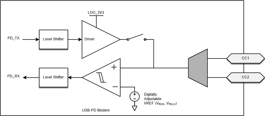
The TPS25730 transmits and receives USB-PD data over one of the CCy pins for a given CC pin pair (one pair per USB Type-C port). The CCy pins are also used to determine the cable orientation and maintain the cable/device attach detection. Thus, a DC bias exists on the CCy pins. The transmitter driver overdrives the CCy DC bias while transmitting, but returns to a Hi-Z state, allowing the DC voltage to return to the CCy pin when it is not transmitting. While either CC1 or CC2 can be used for transmitting and receiving, during a given connection only, the one that mates with the CC pin of the plug is used, so there is no dynamic switching between CC1 and CC2. Figure 8-7 shows the USB-PD BMC TX and RX driver block diagram.
 Figure 8-7 USB-PD
BMC TX/Rx Block Diagram
Figure 8-7 USB-PD
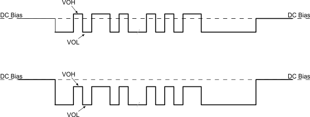
BMC TX/Rx Block DiagramFigure 8-8 shows the transmission of the BMC data on top of the DC bias. Note that the DC bias can be anywhere between the minimum and maximum threshold for detecting a Sink attach. This note means that the DC bias can be above or below the VOH of the transmitter driver.
 Figure 8-8 TX Driver Transmission with DC Bias
The transmitter drives a digital signal onto the CCy lines. The signal peak, VTXHI, is set to meet the TX masks defined in the USB-PD Specifications. Note that the TX mask is measured at the far-end of the cable.
When driving the line, the transmitter driver has an output impedance of ZDRIVER. ZDRIVER is determined by the driver resistance and the shunt capacitance of the source and is frequency dependent. ZDRIVER impacts the noise ingression in the cable.
Figure 8-9 shows the simplified circuit determining ZDRIVER. It is specified such that noise at the receiver is bounded.
 Figure 8-9 ZDRIVER Circuit