SLVSCR1C September   2015  – July 2017 TPS25810

PRODUCTION DATA.  

  1. Features
  2. Applications
  3. Description
  4. Revision History
  5. Pin Configuration and Functions
  6. Specifications
    1. 6.1 Absolute Maximum Ratings
    2. 6.2 ESD Ratings
    3. 6.3 Recommended Operating Conditions
    4. 6.4 Thermal Information
    5. 6.5 Electrical Characteristics
    6. 6.6 Switching Characteristics
    7. 6.7 Typical Characteristics
  7. Detailed Description
    1. 7.1 Overview
      1. 7.1.1 USB Type C Basic
      2. 7.1.2 Configuration Channel
      3. 7.1.3 Detecting a Connection
    2. 7.2 Functional Block Diagram
    3. 7.3 Feature Description
      1. 7.3.1 Configuration Channel Pins CC1 and CC2
      2. 7.3.2 Current Capability Advertisement and Overload Protection
      3. 7.3.3 Undervoltage Lockout (UVLO)
        1. 7.3.3.1  Device Power Pins (IN1, IN2, AUX, OUT, and GND)
        2. 7.3.3.2  FAULT Response
        3. 7.3.3.3  Thermal Shutdown
        4. 7.3.3.4  REF
        5. 7.3.3.5  Audio Accessory Detection
        6. 7.3.3.6  Debug Accessory Detection
        7. 7.3.3.7  Plug Polarity Detection
        8. 7.3.3.8  Device Enable Control
        9. 7.3.3.9  Load Detect
        10. 7.3.3.10 Power Wake
        11. 7.3.3.11 Port Power Management (PPM)
        12. 7.3.3.12 Implementing PPM in a System with Two Type-C Ports
        13. 7.3.3.13 PPM Operation
    4. 7.4 Device Functional Modes
  8. Application and Implementation
    1. 8.1 Application Information
    2. 8.2 Typical Applications
      1. 8.2.1 Type C DFP Port Implementation without BC 1.2 Support
        1. 8.2.1.1 Design Requirements
          1. 8.2.1.1.1 Input and Output Capacitance
        2. 8.2.1.2 Detailed Design Procedure
        3. 8.2.1.3 Application Curves
      2. 8.2.2 Type-C DFP Port Implementation with BC 1.2 (DCP Mode) Support
        1. 8.2.2.1 Design Requirements
        2. 8.2.2.2 Detailed Design Procedure
        3. 8.2.2.3 Application Curves
  9. Power Supply Recommendations
  10. 10Layout
    1. 10.1 Layout Guidelines
    2. 10.2 Layout Example
  11. 11Device and Documentation Support
    1. 11.1 Device Support
      1. 11.1.1 Third-Party Products Disclaimer
    2. 11.2 Documentation Support
      1. 11.2.1 Related Documentation
    3. 11.3 Receiving Notification of Documentation Updates
    4. 11.4 Community Resources
    5. 11.5 Trademarks
    6. 11.6 Electrostatic Discharge Caution
    7. 11.7 Glossary
  12. 12Mechanical, Packaging, and Orderable Information

Package Options

Mechanical Data (Package|Pins)
Thermal pad, mechanical data (Package|Pins)
Orderable Information

Pin Configuration and Functions

RVC Package
20-Pin WQFN
Top View
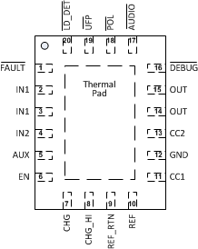
TPS25810 PO2_slvscr1.gif

Pin Functions

PIN I/O DESCRIPTION
NAME NUMBER
FAULT 1 O Fault event indicator. Open-drain logic output that asserts low to indicate current limit or thermal shutdown event due to over temperature.
IN1 2, 3 I VBUS input supply. Internal power switch connects IN1 to OUT.
IN2 4 I VCONN input supply. Internal power switch connects IN2 to CC1 or CC2. Short to IN1 if only one supply is used.
AUX 5 I Auxiliary input supply. Connect to always alive system rail to use the Power Wake feature. Short to IN1 and IN2 if only one supply is used.
EN 6 I Enable logic input to turn the device on and off.
CHG 7 I Charge logic input to select between standard USB (500 mA for a Type C receptacle supporting only USB 2.0 and 900 mA for Type C receptacle supporting USB 3.1) or Type-C current sourcing ability.
CHG_HI 8 I High-charge logic input to select between 1.5-A and 3-A Type-C current sourcing capability. Valid when CHG is set to Type-C current.
REF_RTN 9 I Precision signal reference return. Connect to REF pin via 100-kΩ, 1% resistor.
REF 10 I Analog input used to generate internal current reference. Connect a 1% or better, 100 ppm, 100-kΩ resistor between this pin and REF_RTN.
CC1 11 I/O Analog input/output that connects to the Type-C receptacle CC1 pin
GND 12 Power ground
CC2 13 I/O Analog input/output that connects to the Type-C receptacle CC2 pin.
OUT 14,15 O Power switch output.
DEBUG 16 O Open-drain logic output that asserts when a Type-C Debug accessory is identified on the CC lines.
AUDIO 17 O Open-drain logic output that asserts when a Type-C Audio accessory is identified on the CC lines.
POL 18 O Polarity open-drain logic output that signals which Type-C CC pin is connected to the CC line. This gives the information needed to mux the super speed lines. Asserted when the CC2 pin is connected to the CC line in cable.
UFP 19 O Open-drain logic output that asserts when a Type-C UFP is identified on the CC lines.
LD_DET 20 O Load-detect open-drain logic output that signals when a device set to source Type-C 3 A current is sourcing over 1.95 A nominal.
Thermal Pad Thermal pad on bottom of package.