SLVSCE1C August   2014  – November 2015 TPS25921A , TPS25921L

PRODUCTION DATA.  

  1. Features
  2. Applications
  3. Description
  4. Application Schematic
  5. Revision History
  6. Pin Configuration and Functions
  7. Specifications
    1. 7.1 Absolute Maximum Ratings
    2. 7.2 ESD Ratings
    3. 7.3 Recommended Operating Conditions
    4. 7.4 Thermal Characteristics
    5. 7.5 Electrical Characteristics
    6. 7.6 Timing Requirements
    7. 7.7 Typical Characteristics
  8. Parametric Measurement Information
  9. Detailed Description
    1. 9.1 Overview
    2. 9.2 Functional Block Diagram
    3. 9.3 Feature Description
      1. 9.3.1 Enable and Adjusting Undervoltage Lockout (UVLO)
      2. 9.3.2 Overvoltage Protection (OVP)
      3. 9.3.3 Hot Plug-in and In-Rush Current Control
      4. 9.3.4 Overload and Short Circuit Protection :
        1. 9.3.4.1 Overload Protection
        2. 9.3.4.2 Short Circuit Protection
        3. 9.3.4.3 Start-Up with Short on Output
        4. 9.3.4.4 Constant Current Limit Behavior during Overcurrent Faults
      5. 9.3.5 FAULT Response
      6. 9.3.6 IN, OUT and GND Pins
      7. 9.3.7 Thermal Shutdown:
    4. 9.4 Device Functional Modes
      1. 9.4.1 Shutdown Control
      2. 9.4.2 Operational Overview of Device Functions
  10. 10Applications and Implementation
    1. 10.1 Application Information
    2. 10.2 Typical Application
      1. 10.2.1 Precision Current Limiting and Protection for White Goods
        1. 10.2.1.1 Design Requirements
        2. 10.2.1.2 Detailed Design Procedure
          1. 10.2.1.2.1 Step by Step Design Procedure
          2. 10.2.1.2.2 Programming the Current-Limit Threshold: R(ILIM) Selection
          3. 10.2.1.2.3 Undervoltage Lockout and Overvoltage Set Point
          4. 10.2.1.2.4 Setting Output Voltage Ramp time (tSS)
            1. 10.2.1.2.4.1 Case1: Start-up Without Load: Only Output Capacitance C(OUT) Draws Current During Start-up
            2. 10.2.1.2.4.2 Case 2: Start-up With Load: Output Capacitance C(OUT) and Load Draws Current During Start-up
          5. 10.2.1.2.5 Support Component Selections - R4 and CIN
        3. 10.2.1.3 Application Curves
    3. 10.3 System Examples
      1. 10.3.1 Protection and Current Limiting for Primary-Side Regulated Power Supplies
      2. 10.3.2 Precision Current Limiting in Intrinsic Safety Applications
      3. 10.3.3 Smart Load Switch
  11. 11Power Supply Recommendations
    1. 11.1 Transient Protection
    2. 11.2 Output Short-Circuit Measurements
  12. 12Layout
    1. 12.1 Layout Guidelines
    2. 12.2 Layout Example
  13. 13Device and Documentation Support
    1. 13.1 Related Links
    2. 13.2 Community Resources
    3. 13.3 Trademarks
    4. 13.4 Electrostatic Discharge Caution
    5. 13.5 Glossary
  14. 14Mechanical, Packaging, and Orderable Information

Package Options

Mechanical Data (Package|Pins)
Thermal pad, mechanical data (Package|Pins)
Orderable Information

8 Parametric Measurement Information
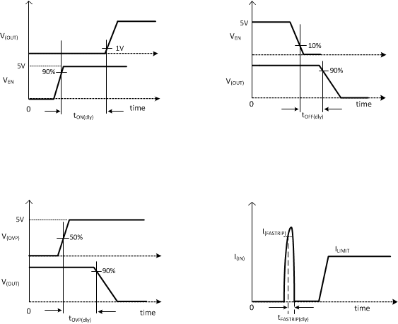
TPS25921A TPS25921L Timing_Diagram_slvsce1.gif Figure 25. Timing Diagrams