SLVSCE9D June 2014 – October 2017 TPS25942A , TPS25942L , TPS25944A , TPS25944L
UNLESS OTHERWISE NOTED, this document contains PRODUCTION DATA.
- 1 Features
- 2 Applications
- 3 Description
- 4 Revision History
- 5 Device Comparison Table
- 6 Pin Configuration and Functions
- 7 Specifications
- 8 Parameter Measurement Information
-
9 Detailed Description
- 9.1 Overview
- 9.2 Functional Block Diagram
- 9.3
Feature Description
- 9.3.1 Enable and Adjusting Undervoltage Lockout
- 9.3.2 Overvoltage Protection (OVP)
- 9.3.3 Hot Plug-In and In-Rush Current Control
- 9.3.4 Overload and Short Circuit Protection
- 9.3.5 Reverse Current Protection
- 9.3.6 FAULT Response
- 9.3.7 Current Monitoring
- 9.3.8 Power Good Comparator
- 9.3.9 IN, OUT and GND Pins
- 9.3.10 Thermal Shutdown
- 9.4 Device Functional Modes
-
10Application and Implementation
- 10.1 Application Information
- 10.2
Typical Application
- 10.2.1 Design Requirements
- 10.2.2
Detailed Design Procedure
- 10.2.2.1 Step by Step Design Procedure
- 10.2.2.2 Programming the Current-Limit Threshold: R(ILIM) Selection
- 10.2.2.3 Undervoltage Lockout and Overvoltage Set Point
- 10.2.2.4 Programming Current Monitoring Resistor—RIMON
- 10.2.2.5 Setting Output Voltage Ramp Time (tdVdT)
- 10.2.2.6 Programing the Power Good Set Point
- 10.2.2.7 Support Component Selections—R6, R7 and CIN
- 10.2.3 Application Curves
- 10.3 System Examples
- 11Power Supply Recommendations
- 12Layout
- 13Device and Documentation Support
- 14Mechanical, Packaging, and Orderable Information
Package Options
Mechanical Data (Package|Pins)
- RVC|20
Thermal pad, mechanical data (Package|Pins)
- RVC|20
Orderable Information
9.3.3 Hot Plug-In and In-Rush Current Control
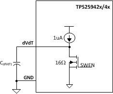
The device is designed to control the in-rush current upon insertion of a card into a live backplane or other "hot" power source. This limits the voltage sag on the backplane’s supply voltage and prevents unintended resets of the system power. A slew rate controlled start-up (dVdT) also helps to eliminate conductive and radiative interferences. An external capacitor connected from the dVdT pin to GND defines the slew rate of the output voltage at power-on (as shown in Figure 51). Equation governing slew rate at start-up is shown in Equation 1.
 Figure 51. Output Ramp Up Time tdVdT is Set by C(dVdT)
where
- I(dVdT) = 1 µA (typical)
 = Desired output slew rate
- GAIN(dVdT) = dVdT to OUT gain = 12
The total ramp time (tdVdT) of V(OUT) for 0 to V(IN) can be calculated using Equation 2.
The inrush current, I(INRUSH) can be calculated as shown in Equation 3.
The dVdT pin can be left floating to obtain a predetermined slew rate (tdVdT) on the output. When terminal is left floating, the device sets an internal ramp rate of 30 V/ms for output (V(OUT)) ramp.
Figure 61 and Figure 62 illustrate the inrush current control behavior of the TPS25942, TPS25944. For systems where load is present during start-up, the current never exceeds the overcurrent limit set by R(ILIM) resistor for the application. For defining appropriate charging time/rate under different load conditions, see the Setting Output Voltage Ramp Time (tdVdT) section.