SLVSDZ4D February 2018 – February 2020 TPS2HB35-Q1
PRODUCTION DATA.
- 1 Features
- 2 Applications
- 3 Description
- 4 Revision History
- 5 Device Comparison Table
- 6 Pin Configuration and Functions
- 7 Specifications
- 8 Parameter Measurement Information
-
9 Detailed Description
- 9.1 Overview
- 9.2 Functional Block Diagram
- 9.3
Feature Description
- 9.3.1 Protection Mechanisms
- 9.3.2 Diagnostic Mechanisms
- 9.4 Device Functional Modes
- 10Application and Implementation
- 11Power Supply Recommendations
- 12Layout
- 13Device and Documentation Support
- 14Mechanical, Packaging, and Orderable Information
Package Options
Mechanical Data (Package|Pins)
- PWP|16
Thermal pad, mechanical data (Package|Pins)
- PWP|16
Orderable Information
10.2.3 Application Curves
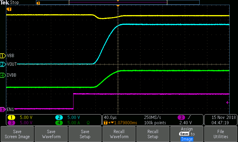
When the device receives a rising edge on the ENx pulse the output will turn on as shown in Figure 52. After the turn-on delay time, the device VOUT goes to the VBB supply and begins outputting the steady state resistive current.
 Figure 52. Turn-On Waveform
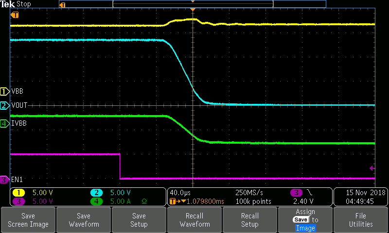
 When the device turns off on a falling edge of ENx, the channel IOUT will go to zero and the VOUT will drop to zero as well as shown in Figure 53.
 Figure 53. Turn-Off Waveform
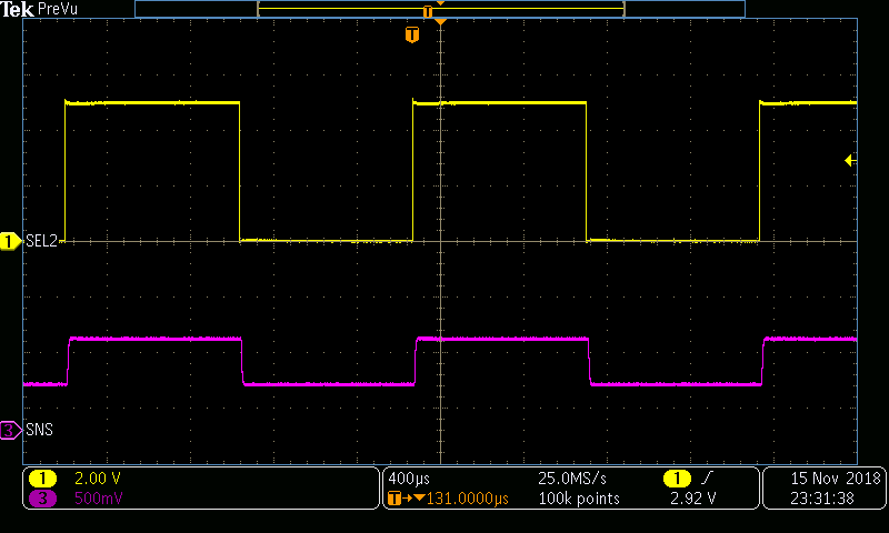
 While enabled, it is important to measure the output current through both channels. Figure 54 shows this behavior when toggling the SELx pins. The image shows that when SEL2 toggles high to low, the SNS pin toggles between representing IOUT1 and IOUT2. When SEL2 is low SNS represents IOUT1 and when SEL2 is high SNS represents IOUT2. This image shows that channel 2 is currently outputting twice the output current as channel 1.
 Figure 54. Toggling Between CH1 and CH2 Current Measurement
 If the output of the TPS2HB35-Q1 is short-circuited, the device will protect the system from failure. shows the device turning off the output at a set current limit when the output is short circuited. (Note: shows a case with a higher RILIM than calculated in this example, so the current limit is higher than 8 A ).
The TPS2HB35-Q1 also has a variant that allows the current to remain on when the current threshold is reached. This allow capacitors to be charged up in one attempt instead of hitting the current limit and immediately shutting down. The short circuit behavior can be seen in Figure 55
 - STG - OTPC_U09_CH2_8p25K_Lin_5uH_Lout_5uH_VBB_13p5V.png) Figure 55. TPS2HB35C-Q1 Short Circuit Waveform
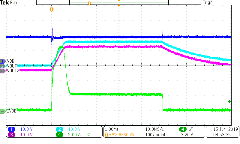
Figure 55. TPS2HB35C-Q1 Short Circuit Waveform Figure 56 shows the TPS2HB35C-Q1 device charging up a 270-µF capacitor in parallel with a 6-Ω resistor to 16 V at 85ºC on both channels. The current waveform is the combined current going through both channels.
 Figure 56. TPS2HB35C-Q1 Charging a 270-µF Capacitor