SLVS227F August 1999 – December 2020
PRODUCTION DATA
- 1Features
- 2Applications
- 3Description
- 4Revision History
- 5Device Comparison
- 6Pin Configuration and Functions
- 7Specifications
- 8Detailed Description
- 9Device and Documentation Support
Package Options
Refer to the PDF data sheet for device specific package drawings
Mechanical Data (Package|Pins)
- DBV|5
Thermal pad, mechanical data (Package|Pins)
Orderable Information
6 Pin Configuration and Functions
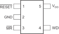
 Figure 6-1 TPS3123
/ TPS3128: DBV PACKAGE
Figure 6-1 TPS3123
/ TPS3128: DBV PACKAGE5-Pin SOT-23
Top View
 Figure 6-3 TPS3125
/ TPS3126: DBV PACKAGE
Figure 6-3 TPS3125
/ TPS3126: DBV PACKAGE5-Pin SOT-23
Top View
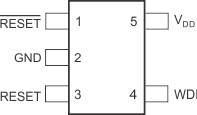
 Figure 6-2 TPS3124: DBV PACKAGE
5-Pin SOT-23
Top View
Table 6-1 Pin Functions
| PIN | I/O | DESCRIPTION | |||
|---|---|---|---|---|---|
| PIN NUMBER | TPS3123 TPS3128 |
TPS3124 | TPS3125 TPS3126 |
||
| 1 | RESET | RESET | RESET | O | Active-Low Output Reset Signal: This pin is driven to a logic low when VDD voltage falls below the negative voltage threshold (VIT-). RESET remains low (asserted) for the delay time period (tD) after VDD voltage rises above VIT+ = VIT- + VHYS. |
| 2 | GND | GND | GND | - | GROUND |
| 3 | MR | - | - | I | Manual Reset: Pull this pin to a logic low to assert a reset signal in the RESET output pin. After MR pin is left floating or pulls to logic high, the RESET output deasserts to the nominal state after the reset delay time (tD) expires. |
| 3 | - | RESET | RESET | O | Active-High Output Reset Signal: This pin is driven to a logic high when VDD voltage falls below the negative voltage threshold (VIT-). RESET remains high (asserted) for the delay time period (tD) after VDD voltage rises above VIT+ = VIT- + VHYS. |
| 4 | WDI | WDI | MR | I | Watchdog timer input: If WDI remains high or low longer than the timeout period, then reset is triggered. The timer clears when reset is asserted or when WDI sees a rising edge or a falling edge. If unused, the WDI connection must be high impedance to prevent it from causing a reset event. |
| 5 | VDD | VDD | VDD | I | Input Supply Voltage: Supply voltage pin. Good analog design practice is to place a 0.1-µF ceramic capacitor close to this pin. |