SBVS211B August 2012 – April 2015
PRODUCTION DATA.
- 1 Features
- 2 Applications
- 3 Description
- 4 Revision History
- 5 Pin Configuration and Functions
- 6 Specifications
- 7 Detailed Description
- 8 Application and Implementation
- 9 Power Supply Recommendations
- 10Layout
- 11Device and Documentation Support
- 12Mechanical, Packaging, and Orderable Information
Package Options
Mechanical Data (Package|Pins)
- DRY|6
Thermal pad, mechanical data (Package|Pins)
- DRY|6
Orderable Information
8 Application and Implementation
NOTE
Information in the following applications sections is not part of the TI component specification, and TI does not warrant its accuracy or completeness. TI’s customers are responsible for determining suitability of components for their purposes. Customers should validate and test their design implementation to confirm system functionality.
8.1 Application Information
The TPS342x family of devices are small, low-current, push-button reset timers. These devices use a long timing setup delay to provide the system reset signals, and avoid resets from short push-button closures. This reset configuration allows for differentiation between user inputs and hard system resets. TPS342x uses an open drain output, has an input voltage range of 1.6 V to 6.5 V, and is specified from –40°C to +125°C.
The TPS3420 and TPS3421 are used to monitor two inputs while TPS3422 is used to monitor a single input.
8.2 Typical Applications
8.2.1 Single Input With Fixed Reset Pulse Duration
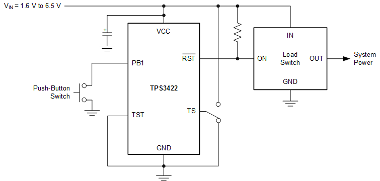
If only one input must be monitored to set the state of a logic pin, such as the enable pin of a load switch, use the TPS3422. After a reset event has occurred, RST is held low for a fixed amount of time (tRST) regardless of the state of the PB1 pin.
An application diagram is shown in Figure 15.
8.2.1.1 Design Requirements
Table 3 lists the design requirements for Figure 15.
Table 3. Design Requirements and Results
| DESIGN REQUIREMENTS | DESIGN RESULT |
|---|---|
| Single input | PB1 |
| Does not react to input signal less than 5 s | 6 s (minimum) |
| Reset pulse greater than 240 ms | 320 ms (minimum) |
| ICC < 5 µA | 3.3 μA (maximum) |
8.2.1.2 Detailed Design Procedure
When the output switches to the high-Z state, the rise time of the RST node depends on the pullup resistance and the capacitance on that node. Choose pullup resistors that satisfy both the downstream timing requirements and the sink current required to have a VOL low enough for the application; 1-kΩ to 1-MΩ resistors are a good choice for low-capacitive loads.
8.2.1.3 Application Curve
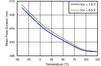 Figure 16. Reset Pulse Duration vs Temperature
8.2.2 Dual Input Applications
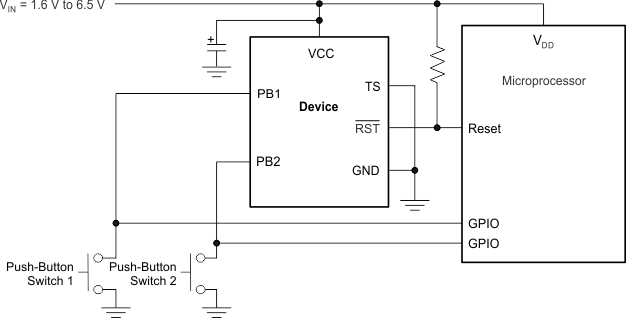
If two inputs must be monitored to set the state of a microprocessor reset pin, either the TPS3420 or the TPS3421 can be used. The system functionality determines which device to use. Use the TPS3420 if RST must be held low until the signal on one of the PBx pins transitions to a logic high state. Use the TPS3421 if RST should only be held low for a fixed amount of time (tRST) regardless of the state of the PBx pins.
An application diagram that is suitable for either the TPS3420 and the TPS3421 is shown in Figure 17.
8.2.2.1 Design Requirements
Table 4 lists the design requirements for Figure 17.
Table 4. Design Requirements and Results
| DESIGN REQUIREMENTS | DESIGN RESULT | |
|---|---|---|
| TPS3420 | TPS3421 | |
| Dual input | PB1 and PB2 | PB1 and PB2 |
| Does not react to input signal less than 5 s | 6 s (minimum) | 6 s (minimum) |
| Reset pulse greater than 140 ms | Depends on PBx timing | 320 ms (minimum) |
| Reset pulse ends after at least one input goes high | True | Does not depend on PBx timing |
8.2.2.2 Detailed Design Procedure
Determine which version of the TPS342x family best suits the functional performance required.
When the output switches to the high-Z state, the rise time of the RST node depends on the pullup resistance and the capacitance on that node. Choose pullup resistors that satisfy both the downstream timing requirements and the sink current required to have a VOL low enough for the application; 1-kΩ to 1-MΩ resistors are a good choice for low-capacitive loads.
8.2.2.3 Application Curve
 Figure 18. Reset Pulse Duration vs Temperature
8.2.3 Latched Reset Signal
Some applications require the reset signal (RST) to be latched and only change state after a second low input signal is received. To achieve a latched version of the RST signal, a D-flip-flop can be used. The output of the D-flip-flop, Q, is then connected to the device to be reset.
See Figure 19 for an example of a latched reset signal configuration.
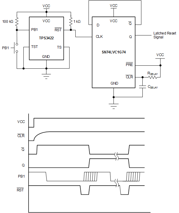 Figure 19. Latched Reset Schematic and Timing Diagram
8.2.3.1 Design Requirements
Table 5 summarizes the design requirements for Figure 19.
Table 5. Design Requirements and Results
| DESIGN REQUIREMENTS | DESIGN RESULT |
|---|---|
| Single input | PB1 |
| Latched output | Q |
| Does not react to input signal less than 5 s | 6 s (minimum) |
| Reset pulse greater than 200 ms | 320 ms (minimum) |
| ICC < 20 µA | 13.3 μA (maximum) |
8.2.3.2 Detailed Design Procedure
Once a positive-edge triggered D-flip-flop is chosen, make sure the slew rate of the RST signal is fast enough to trigger the flip-flop. For the SN74LVC1G74 shown in Figure 19, TI recommends a 1-kΩ pullup resistor. The RC time constant of the delay cap (CDELAY) and delay resistor (RDELAY)should be 10 times the rise time of the input voltage to VCC so that a clear signal is sent to the D-flip-flop, to initialize it into a known state.
8.2.3.3 Application Curve
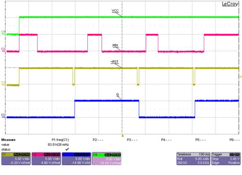 Figure 20. Latched Reset Waveforms Using SN74LVC1G74