SBVS240C November   2014  – February 2019 TPS3701

PRODUCTION DATA.  

  1. Features
  2. Applications
  3. Description
    1.     Device Images
      1.      Typical Application
      2.      Typical Error vs Junction Temperature
  4. Revision History
  5. Pin Configuration and Functions
    1.     Pin Functions
  6. Specifications
    1. 6.1 Absolute Maximum Ratings
    2. 6.2 ESD Ratings
    3. 6.3 Recommended Operating Conditions
    4. 6.4 Thermal Information
    5. 6.5 Electrical Characteristics
    6. 6.6 Timing Requirements
    7. 6.7 Typical Characteristics
  7. Detailed Description
    1. 7.1 Overview
    2. 7.2 Functional Block Diagram
    3. 7.3 Feature Description
      1. 7.3.1 Inputs (INA, INB)
      2. 7.3.2 Outputs (OUTA, OUTB)
    4. 7.4 Device Functional Modes
      1. 7.4.1 Normal Operation (VDD > UVLO)
      2. 7.4.2 Undervoltage Lockout (V(POR) < VDD < UVLO)
      3. 7.4.3 Power-On-Reset (VDD < V(POR))
  8. Application and Implementation
    1. 8.1 Application Information
      1. 8.1.1 Window Voltage Detector Considerations
      2. 8.1.2 Input and Output Configurations
      3. 8.1.3 Immunity to Input Pin Voltage Transients
    2. 8.2 Typical Application
      1. 8.2.1 Design Requirements
      2. 8.2.2 Detailed Design Procedure
      3. 8.2.3 Application Curve
  9. Power Supply Recommendations
  10. 10Layout
    1. 10.1 Layout Guidelines
    2. 10.2 Layout Example
  11. 11Device and Documentation Support
    1. 11.1 Documentation Support
      1. 11.1.1 Related Documentation
    2. 11.2 Receiving Notification of Documentation Updates
    3. 11.3 Community Resources
    4. 11.4 Trademarks
    5. 11.5 Electrostatic Discharge Caution
    6. 11.6 Glossary
  12. 12Mechanical, Packaging, and Orderable Information

Package Options

Mechanical Data (Package|Pins)
Thermal pad, mechanical data (Package|Pins)
Orderable Information

Typical Characteristics

At TJ = 25°C and VDD = 12 V, unless otherwise noted.
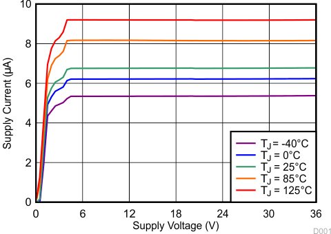
TPS3701 D001_sbvs240.gif
Figure 2. Supply Current vs Supply Voltage
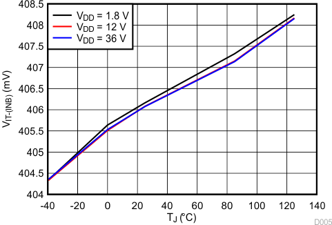
TPS3701 D005_sbvs240.gifFigure 4. INA Positive Input Threshold Voltage (VIT+(INA)) vs Temperature
TPS3701 D004_sbvs240.gif
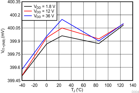
Figure 6. INB Positive Input Threshold Voltage (VIT+(INB)) vs Temperature
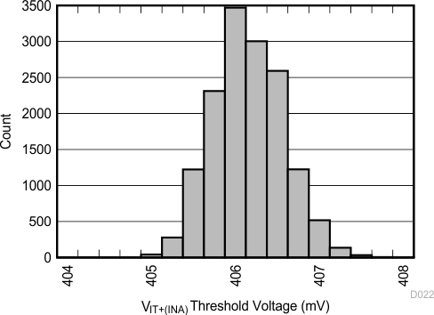
TPS3701 D022_sbvs240.gif
VDD = 1.8 V
Figure 8. INA Positive Input Threshold Voltage (VIT+(INA)) Distribution
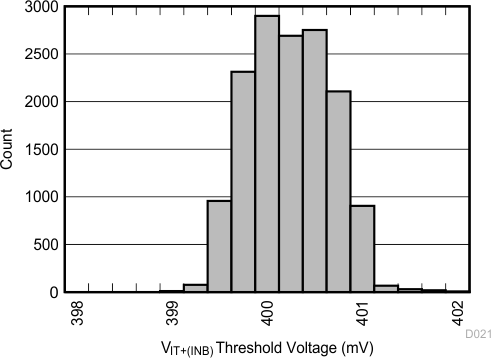
TPS3701 D021_sbvs240.gif
VDD = 1.8 V
Figure 10. INB Positive Input Threshold Voltage (VIT+(INB)) Distribution
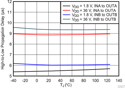
TPS3701 D007_sbvs240.gif
Input step ±200 mV
Figure 12. Propagation Delay vs Temperature
(High-to-Low Transition at the Inputs)
TPS3701 D009_sbvs240.gif
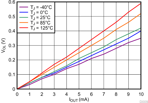
VDD = 1.8 V
Figure 14. Output Voltage Low vs Output Sink Current
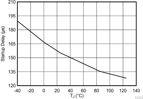
TPS3701 D025_sbvs240.gif
VDD = 5 V
Figure 16. Start-Up Delay vs Temperature
TPS3701 StartupDelay4.gif
VDD = 5 V, VINA = 410 mV, VINB = 390 mV, VPULL-UP = 3.3 V
Figure 18. Start-Up Delay
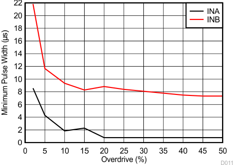
TPS3701 D011_sbvs240.gif
VDD = 24 V
Figure 3. Minimum Pulse Duration vs
Threshold Overdrive Voltage(1)(1)
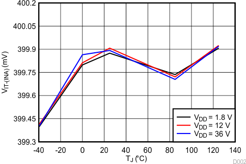
TPS3701 D002_sbvs240.gifFigure 5. INA Negative Input Threshold Voltage (VIT–(INA)) vs Temperature
TPS3701 D003_sbvs240.gif
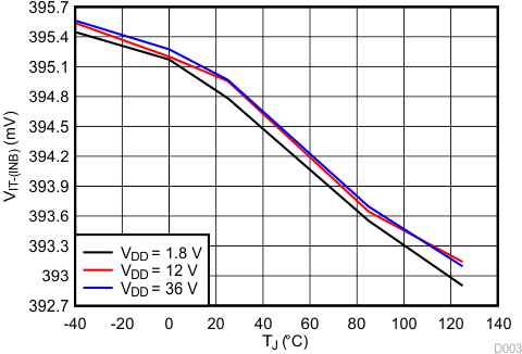
Figure 7. INB Negative Input Threshold Voltage (VIT–(INB)) vs Temperature
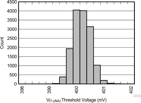
TPS3701 D020_sbvs240.gif
VDD = 1.8 V
Figure 9. INA Negative Input Threshold Voltage (VIT–(INA)) Distribution
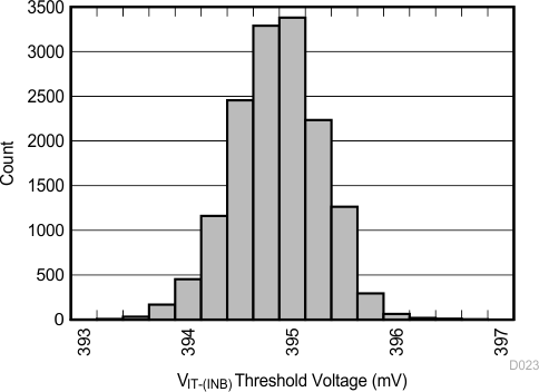
TPS3701 D023_sbvs240.gif
VDD = 1.8 V
Figure 11. INB Negative Input Threshold Voltage (VIT–(INB)) Distribution
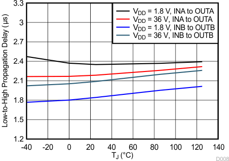
TPS3701 D008_sbvs240.gif
Input step ±200 mV
Figure 13. Propagation Delay vs Temperature
(Low-to-High Transition at the Inputs)
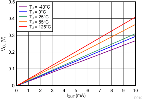
TPS3701 D010_sbvs240.gif
VDD = 12 V
Figure 15. Output Voltage Low vs Output Sink Current
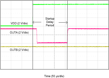
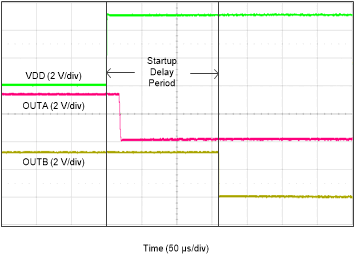
TPS3701 StartupDelay5.gif
VDD = 5 V, VINA = 390 mV, VINB = 410 mV, VPULL-UP = 3.3 V
Figure 17. Start-Up Delay
Minimum pulse duration required to trigger output high-to-low transition. INA = negative spike below VIT– and INB = positive spike above VIT+.